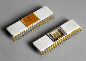
The Intel 8080 is a seminal CPU introduced in 1974 that gave rise to the personal computer/home computer/microcomputer revolution.
It was integrated in early home computers like the Altair 8800, the Interact Home Computer, the DAI Personal Computer, and arcade systems like the Taito 8080 and Midway 8080.
History
The 8080 is often said to be the "first truly usable microprocessor". This CPU is 10 times faster than its predecessor, the Intel 8008 issued in 1972.
The 8008 had, among other limitations, a rigid seven-level address call stack instead of a flexible Stack Pointer. The 8008 instruction set was itself based on the CPU board, built out of dozens of TTL chips, of the Datapoint 2200 computer. Source
Despite what their naming suggest, the Intel 8008 and Intel 4004 were separate projects with distinct architectures and purposes. The 8008 was not an upgrade or evolution of the 4004. The die shot of the 4004 reveals the initials FF of the chip designer, Federico Faggin. The die shot of the 8008 reveals the initials HF of the chip designer, Hal Feeney.
See: Die photos and analysis The ALU The counters The carry-lookahead circuit 8008 microprocessor reverse engineered
Fun fact: Before microprocessors were invented, there was already ALU chips, like the 74181 ALU chip, that were used in CPU boards Source. And creating a 16-bit ALU was just a matter of combining four 74181 ALU chips with a 74182 lookahead carry chip Source.
Technology
The 8008 was built with PMOS circuitry, while the 8080 was built with NMOS, which provided much superior performance.
NMOS became the standard microprocessor technology until the rise of CMOS in the 1980s, combining NMOS and PMOS to dramatically reduce power consumption.
Compatibility
The 8080 is not binary-compatible with the 8008 because almost all the instructions were shifted to different opcodes.
One important but subtle change was that the 8 register/memory codes were reordered to start with B instead of A. The motivation is that this gave registers in a 16-bit register pair (BC, DE, or HL) codes that differ only in the low bit. This makes it easier to specify a register pair with a two-bit code.
CP/M required an 8080, 8085 or Z80 CPU and between 1976 and about 1983, microcomputers with a Z80 that ran CP/M were the norm before the market shifted to MS-DOS.
Register File
| Register | Size | Description | Notes |
|---|---|---|---|
| B, C, D, E, H, L | 8-bit | General-purpose registers | Can be used individually or as 16-bit pairs: BC, DE, HL |
| A (Accumulator) | 8-bit | Primary register for arithmetic, logic, and data transfer operations | Often the destination or source for operations |
| F (Flags) | 8-bit | Status flags reflecting results of operations:
|
HF is used for BCD arithmetic (DAA instruction).
The accumulator and the flags together are called the PSW, or program status word. PSW can be pushed to or popped from the stack. |
| SP (Stack Pointer) | 16-bit | Points to the top of the stack | Used for PUSH, POP, CALL, RET instructions |
| PC (Program Counter) | 16-bit | Points to the memory address of the next instruction byte to be fetched | Increments automatically after fetching instruction bytes |
Instruction Cycle
Just like the Z80, the 8080 is composed of M-cycles and T-states.
Each ctock period marks a state; 3 to 5 states constitute a machine cycle; and 1 to 5 machine cycles comprise an instruction cycle.
A full instruction cycle requires anywhere from 4 to 18 states for its completion, depending on the kind of instruction involved.
| T-state | Description |
|---|---|
| T1 | A memory address or I/O device number is placed on the Address Bus (A15-0); status information is placed on Data Bus (D7-0). |
| T2 | The CPU samples the READY and HOLD inputs and checks for halt instruction. |
| TW (optional) | Processor enters wait state if READY is low or if HALT instruction has been executed. |
| T3 | An instruction byte (FETCH machine cycle), data byte (MEMORY READ, STACK READ) or interrupt instruction (INTERRUPT machine cycle) is input to the CPU from the Data Bus; or a data byte (MEMORY WRITE, STACK WRITE or OUTPUT machine cycle) is output onto the data bus. |
| T4, T5 (optional) | States T4 and T5 are available if the execution of a particular instruction requires them; if not, the CPU may skip one or both of them. T4 and T5 are only used for internal processor operations. |
See this Intel 8080 document, containing a detailed breakdown of M-cycles and T-states.
Block Diagram
Evolution
The 8080 ultimately led to the machine code-compatible, but more powerful clone Zilog Z80, which was used in the Amstrad CPC and Sinclair ZX Spectrum among others.
However, because Intel claimed a copyright on their assembly mnemonics, Zilog had to develop a new assembly syntax for the Z80 (e.g. the Z80 uses LD whereas the 8080 has MOV and several other commands). See Mapping between i8080 and Z80 mnemonics
Meanwhile Intel produced the 8085, an improved, backward-compatible version of the 8080, with refinements to power consumption and integration. i8085 compatibility grid with Z80 & GBZ80
See: Notes on PLA Inside the ALU Instruction set: the octal table Register file Flag circuits The ALU and its hidden registers Decimal adjust circuitry 8085 CPU reverse engineered
Links
- Intel 8080 at the English-language Wikipedia
- Intel 8080A datasheet
- 8080 Systems User's Manual
- 8080 assembly language programming manual
- 8080 opcode map
- 8080 CPU Exerciser
- Intel 4004 Intel 8008 Intel 8080 Oral history panels


