Difference between revisions of "C't 512 KB internal RAM expansion"
(→Step 2 - Daughterboard Logic) |
|||
| (26 intermediate revisions by 3 users not shown) | |||
| Line 1: | Line 1: | ||
| − | + | [[Category:DIY]] [[Category:Memory expansions]] | |
| + | A project to upgrade a CPC6128 to 512K RAM (total), done by replacing the CPC6128's RAM chips, and its PAL banking chip, the project was released 1987 in german magazine ''c't Magazin''. | ||
| − | + | == The Circuit == | |
| − | + | * '''DRAM Replacement''' - Replace the sixteen old 64Kx1 DRAM chips (IC119-IC134) by new 256Kx1 DRAMs. The chips have same pinouts, only pin 1 is changed (old: NC, new: A8 row:column address signal). Optionally, replace only bank 0 (IC127-IC134) for getting only 320K (256K+64K) instead of 512K total (2x256K). | |
| − | + | * '''PAL Replacement''' - Replace the old PAL (IC118) by the new daughterboard. Most signals connect to the PAL socket (green in schematic), a extra few wires connect elsewhere on mainboard (red), as an optional "bonus" feature, the circuit contains logic for a 3rd floppy drive (blue). | |
| − | + | <gallery> | |
| − | + | File:CPC6512 ct magazin schematic.png|Schematic | |
| − | + | File:CPC6512 ct magazin pcb.jpg|PCB | |
| − | + | </gallery> | |
| − | + | ||
| + | '''Component List''' | ||
16x 41256 (256Kx1 DRAM) ;replacing the CPC6128's 16 built-in 64Kx1 DRAMs | 16x 41256 (256Kx1 DRAM) ;replacing the CPC6128's 16 built-in 64Kx1 DRAMs | ||
| − | 1x PAL 16L8 ;replacing the CPC6128's | + | 1x PAL 16L8 ;replacing the CPC6128's built-in PAL |
| − | 1x 74LS38 | + | 1x 74LS38 ;Quad 2-input NAND, OC |
| − | 1x 74LS273 | + | 1x 74LS273 ;8bit latch, of which only 5bit are used here |
| − | 1x 2200 Ohm resistor | + | 1x 2200 Ohm resistor ;pull-up for OC output |
| − | 1x 470 Ohm resistor | + | 1x 470 Ohm resistor ;pull-up for OC output |
| − | 1x 47 Ohm resistor | + | 1x 47 Ohm resistor ;purpose unknown (noise related? shortcut protection?) |
| − | == | + | == Compatibility Problems == |
| − | The | + | * RAMDIS is not supported, not a problem in most cases, but won't work with some special types of expansion hardware, like [[Multiface II]]. |
| + | * The expansion seems to have been designed independently of [[Standard Memory Expansions]] like the dk'tronics one. So, there is no (intended) compatibility. However, both c't and dk'tronics are designed around the CPC6128 banking mechanism, so they do work similar in some ways. Namely, both can map expansion banks to 4000h..7FFFh, but there are several differences: | ||
| + | ** For the mapping to 4000h..7FFFh, dk'tronics uses values CCh..CFh, D4h..C7h, DCh..DFh, ... FCh..FFh whilst c't uses values C8h..DFh. Some of these values do overlap, resulting in some (unintended) semi-compatibility, but there's still one big difference: along with the above values, dk'tronics maps bank 3 to C000h..FFFFh, whilst c't maps bank 7 to that region. | ||
| − | + | == Memory Configurations == | |
| − | + | ||
| − | + | The memory is controlled by OUT [7Fxxh],C0h..DFh instructions. Values C0h..C7h are working same as on normal CPC6128s. Values C8h..DFh do access the additional RAM banks (C8h..D3h when using the cut-down 320K upgrade variant). | |
| − | + | OUT [7Fxxh],C0h+... 0 1 2 3 4 5 6 7 8..31 | |
| + | ------------------------------------------------------- | ||
| + | Bank at C000h..FFFFh 3 7 7 7 3 3 3 3 7 (!) | ||
| + | Bank at 8000h..BFFFh 2 2 6 2 2 2 2 2 2 | ||
| + | Bank at 4000h..7FFFh 1 1 5 3 4 5 6 7 8..31 | ||
| + | Bank at 0000h..3FFFh 0 0 4 0 0 0 0 0 0 | ||
| − | + | == PAL Source Code == | |
| − | + | Below is a typed-up and commented copy of the PALASM source code from the original article. | |
| − | == | + | D7D6 D0 D3 D4 D1 D2 NCAS A15 A14 GND ;pin 1..10 |
| + | CPU A15S AMUX MUX LCLK CAS1 CAS0 IOWR A14S VCC ;pin 11..20 | ||
| + | |||
| + | IF (VCC) /LCLK= D7D6 * /A15 * /IOWR ;load external latch on OUT [7Fxxh],C0h..FFh | ||
| + | |||
| + | IF (VCC) /CAS0= /NCAS * /D4 + ;bank bit4=0, select bank 0..15 (CPU and CRTC) | ||
| + | /CAS0= /NCAS * A15 + | ||
| + | /CAS0= /NCAS * /A14 + | ||
| + | /CAS0= /NCAS * CPU | ||
| + | |||
| + | IF (VCC) /CAS1= /NCAS * D4 * /A15 * A14 * /CPU ;bank bit4=1, select bank 16..31 (CPU at 4000h..7FFFh only) | ||
| + | |||
| + | IF (VCC) /A14S= /A14 + ;bank bit0 | ||
| + | /D0 * D2 * /A15 + | ||
| + | /D0 * D3 * /A15 + | ||
| + | /D0 * D4 * /A15 | ||
| + | |||
| + | IF (VCC) /A15S= /A14 * /A15 + ;bank bit1 | ||
| + | /D1 * /A15 + | ||
| + | /D4 * /D3 * /D2 * /D0 * /A15 + | ||
| + | /D4 * /D3 * /D2 * /D1 * /A15 | ||
| + | |||
| + | IF (VCC) /AMUX= /D0 * D1 * /D2 * /D3 * /D4 * /CPU * /MUX + | ||
| + | A15 * A14 * /D2 * D0 * /CPU * /MUX + | ||
| + | A15 * A14 * /D2 * D1 * /CPU * /MUX + | ||
| + | A15 * A14 * D3 * /CPU * /MUX + | ||
| + | A15 * A14 * D4 * /CPU * /MUX + | ||
| + | /A15 * A14 * D2 * /CPU * /MUX + ;bank bit2 | ||
| + | /A15 * A14 * D3 * /CPU * MUX ;bank bit3 | ||
| + | |||
| + | IF (GND) /MUX = /MUX ;dummy (do not output anything on this pin) | ||
| + | |||
| + | IF (GND) /IOWR=/IOWR ;dummy (do not output anything on this pin) | ||
| − | + | '''Note:''' For VRAM access, bank bits 2,3,4 are forced to zero (by above formulas), bank bit 0,1 are coming from the CRTC, passed directly to IC109 (without going through the PAL), so, the RAM banking affects only the CPU's memory accesses, not the CRTC's video memory accesses. | |
| − | + | ||
| − | + | ||
| − | + | ||
| − | + | ||
| − | + | ||
| − | + | ||
| − | + | ||
| − | + | ||
| − | + | ||
| − | + | ||
| − | + | ||
| − | + | ||
| − | + | ||
| − | + | ||
| − | + | ||
| − | + | ||
| − | * | + | Some notes on the syntax: |
| + | * The first two lines assign the pin-outs. Observe that leading "/" slashes are omitted here. For example, "/CPU" (in schematic) becomes "CPU" (in source code). Accordingly "/CPU" (in source code) would be double-negated "//CPU" aka "CPU" (in schematic). | ||
| + | * The "IF (condition) signal=" part means that "signal" becomes an output when condition is true. In the above source code, condition is always true (VCC), or, for the last 2 lines, always false (GND). | ||
| + | * The "*" and "+" operators are meaning "* = AND", "+ = OR". The idea behind that confusing syntax was to make it "easier" to learn for people who are trained only in basic maths (the formulas do also work when treating *=multiply, and +=plus. For example: 1+0+1+1 = 3 = nonzero = true). | ||
| + | * There must be some priority ordering in the formulas: Either * before +, or operations inside of a line before merging the results of the separate lines (in above examples, both ordering methods do work). | ||
== Scanned Article / Schematics == | == Scanned Article / Schematics == | ||
| − | * [[Media:CPC6512 ct magazin part 1.pdf]] - c't issue 10/1987 - Schematic | + | * [[Media:CPC6512 ct magazin part 1.pdf]] - c't issue 10/1987 - RAM Expansion Schematic |
| − | * [[Media:CPC6512 ct magazin part 2.pdf]] - c't issue 11/1987 - RAM Disc driver | + | * [[Media:CPC6512 ct magazin part 2.pdf]] - c't issue 11/1987 - RAM Disc driver for CP/M Plus |
| − | + | Original names of the articles are: '''Aus David wird Goliath: 512 KB RAM für Schneider CPC''' (part 1), and '''Byte-Hirte: RAM-Disk-Treiber für des CPCs 512 Kbyte''' (part 2). Both articles are written by Gabor Herr and Hubert Schröer. | |
| − | + | == Related hardware modifications == | |
| − | + | ||
| − | + | ||
| − | + | ||
| − | + | ||
| − | |||
* [http://cpcwiki.eu/forum/index.php/topic,662.msg7113.html#msg7113 Bank Swapper by Khany/Cherry-T] (less complex: bank-exchanging toggle, no memory expansion; 1993) | * [http://cpcwiki.eu/forum/index.php/topic,662.msg7113.html#msg7113 Bank Swapper by Khany/Cherry-T] (less complex: bank-exchanging toggle, no memory expansion; 1993) | ||
* [[CPC4MB| CPC4MB memory upgrade by Yarek]] (more advanced; 2005/2006) | * [[CPC4MB| CPC4MB memory upgrade by Yarek]] (more advanced; 2005/2006) | ||
Revision as of 21:23, 16 December 2010
A project to upgrade a CPC6128 to 512K RAM (total), done by replacing the CPC6128's RAM chips, and its PAL banking chip, the project was released 1987 in german magazine c't Magazin.
Contents
The Circuit
- DRAM Replacement - Replace the sixteen old 64Kx1 DRAM chips (IC119-IC134) by new 256Kx1 DRAMs. The chips have same pinouts, only pin 1 is changed (old: NC, new: A8 row:column address signal). Optionally, replace only bank 0 (IC127-IC134) for getting only 320K (256K+64K) instead of 512K total (2x256K).
- PAL Replacement - Replace the old PAL (IC118) by the new daughterboard. Most signals connect to the PAL socket (green in schematic), a extra few wires connect elsewhere on mainboard (red), as an optional "bonus" feature, the circuit contains logic for a 3rd floppy drive (blue).
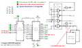
Schematic
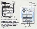
PCB


Component List
 16x 41256 (256Kx1 DRAM)   ;replacing the CPC6128's 16 built-in 64Kx1 DRAMs
  1x PAL 16L8              ;replacing the CPC6128's built-in PAL
  1x 74LS38                ;Quad 2-input NAND, OC
  1x 74LS273               ;8bit latch, of which only 5bit are used here
  1x 2200 Ohm resistor     ;pull-up for OC output
  1x 470 Ohm resistor      ;pull-up for OC output
  1x 47 Ohm resistor       ;purpose unknown (noise related? shortcut protection?)
Compatibility Problems
- RAMDIS is not supported, not a problem in most cases, but won't work with some special types of expansion hardware, like Multiface II.
- The expansion seems to have been designed independently of Standard Memory Expansions like the dk'tronics one. So, there is no (intended) compatibility. However, both c't and dk'tronics are designed around the CPC6128 banking mechanism, so they do work similar in some ways. Namely, both can map expansion banks to 4000h..7FFFh, but there are several differences:
- For the mapping to 4000h..7FFFh, dk'tronics uses values CCh..CFh, D4h..C7h, DCh..DFh, ... FCh..FFh whilst c't uses values C8h..DFh. Some of these values do overlap, resulting in some (unintended) semi-compatibility, but there's still one big difference: along with the above values, dk'tronics maps bank 3 to C000h..FFFFh, whilst c't maps bank 7 to that region.
Memory Configurations
The memory is controlled by OUT [7Fxxh],C0h..DFh instructions. Values C0h..C7h are working same as on normal CPC6128s. Values C8h..DFh do access the additional RAM banks (C8h..D3h when using the cut-down 320K upgrade variant).
 OUT [7Fxxh],C0h+...   0  1  2  3    4  5  6  7    8..31
 -------------------------------------------------------
 Bank at C000h..FFFFh  3  7  7  7    3  3  3  3    7 (!)
 Bank at 8000h..BFFFh  2  2  6  2    2  2  2  2    2
 Bank at 4000h..7FFFh  1  1  5  3    4  5  6  7    8..31
 Bank at 0000h..3FFFh  0  0  4  0    0  0  0  0    0
PAL Source Code
Below is a typed-up and commented copy of the PALASM source code from the original article.
D7D6 D0   D3   D4   D1   D2   NCAS A15  A14  GND  ;pin 1..10
CPU  A15S AMUX MUX  LCLK CAS1 CAS0 IOWR A14S VCC  ;pin 11..20

IF (VCC) /LCLK= D7D6 * /A15 * /IOWR               ;load external latch on OUT [7Fxxh],C0h..FFh

IF (VCC) /CAS0= /NCAS * /D4  +                    ;bank bit4=0, select bank 0..15 (CPU and CRTC)
         /CAS0= /NCAS *  A15 +
         /CAS0= /NCAS * /A14 +
         /CAS0= /NCAS *  CPU

IF (VCC) /CAS1= /NCAS * D4 * /A15 * A14 * /CPU    ;bank bit4=1, select bank 16..31 (CPU at 4000h..7FFFh only)

IF (VCC) /A14S= /A14             +                             ;bank bit0
                /D0  * D2 * /A15 +
                /D0  * D3 * /A15 +
                /D0  * D4 * /A15

IF (VCC) /A15S= /A14 *                    /A15 +               ;bank bit1
                /D1  *                    /A15 +
                /D4  * /D3  * /D2 * /D0 * /A15 +
                /D4  * /D3  * /D2 * /D1 * /A15

IF (VCC) /AMUX= /D0  *  D1  * /D2 * /D3 * /D4 * /CPU * /MUX +
                 A15 *  A14 * /D2 *  D0 *       /CPU * /MUX +
                 A15 *  A14 * /D2 *  D1 *       /CPU * /MUX +
                 A15 *  A14 *        D3 *       /CPU * /MUX +
                 A15 *  A14 *        D4 *       /CPU * /MUX +
                /A15 *  A14 *        D2 *       /CPU * /MUX +  ;bank bit2
                /A15 *  A14 *        D3 *       /CPU *  MUX    ;bank bit3

IF (GND) /MUX = /MUX      ;dummy (do not output anything on this pin)

IF (GND) /IOWR=/IOWR      ;dummy (do not output anything on this pin)
Note: For VRAM access, bank bits 2,3,4 are forced to zero (by above formulas), bank bit 0,1 are coming from the CRTC, passed directly to IC109 (without going through the PAL), so, the RAM banking affects only the CPU's memory accesses, not the CRTC's video memory accesses.
Some notes on the syntax:
- The first two lines assign the pin-outs. Observe that leading "/" slashes are omitted here. For example, "/CPU" (in schematic) becomes "CPU" (in source code). Accordingly "/CPU" (in source code) would be double-negated "//CPU" aka "CPU" (in schematic).
- The "IF (condition) signal=" part means that "signal" becomes an output when condition is true. In the above source code, condition is always true (VCC), or, for the last 2 lines, always false (GND).
- The "*" and "+" operators are meaning "* = AND", "+ = OR". The idea behind that confusing syntax was to make it "easier" to learn for people who are trained only in basic maths (the formulas do also work when treating *=multiply, and +=plus. For example: 1+0+1+1 = 3 = nonzero = true).
- There must be some priority ordering in the formulas: Either * before +, or operations inside of a line before merging the results of the separate lines (in above examples, both ordering methods do work).
Scanned Article / Schematics
- Media:CPC6512 ct magazin part 1.pdf - c't issue 10/1987 - RAM Expansion Schematic
- Media:CPC6512 ct magazin part 2.pdf - c't issue 11/1987 - RAM Disc driver for CP/M Plus
Original names of the articles are: Aus David wird Goliath: 512 KB RAM für Schneider CPC (part 1), and Byte-Hirte: RAM-Disk-Treiber für des CPCs 512 Kbyte (part 2). Both articles are written by Gabor Herr and Hubert Schröer.
Related hardware modifications
- Bank Swapper by Khany/Cherry-T (less complex: bank-exchanging toggle, no memory expansion; 1993)
- CPC4MB memory upgrade by Yarek (more advanced; 2005/2006)