Difference between revisions of "Schneiderware Pseudo ROM"
(→I/O Ports) |
m |
||
| Line 26: | Line 26: | ||
== Software == | == Software == | ||
| − | The magazine article contains three listings with examples how to use the Pseudo ROM board, including a ROM version of the [[Schneiderware Real Time Clock]] driver. | + | The magazine article contains three listings with examples on how to use the Pseudo ROM board, including a ROM version of the [[Schneiderware Real Time Clock]] driver. |
== Scanned Article == | == Scanned Article == | ||
* [[Media:Schneiderware 8 - Pseudo ROM.pdf|Schneiderware 8 - Pseudo ROM.pdf]] - SRAM and EPROM mapped as ROM - '''4/1987 page 26-34''', plus corrections in 5/1987 page 32-34 | * [[Media:Schneiderware 8 - Pseudo ROM.pdf|Schneiderware 8 - Pseudo ROM.pdf]] - SRAM and EPROM mapped as ROM - '''4/1987 page 26-34''', plus corrections in 5/1987 page 32-34 | ||
Revision as of 12:56, 27 August 2011
The Schneiderware Pseudo ROM is a expansion "ROM" board, with 16K EPROM (read-only) and 16K battery-backed SRAM (read/write-able), published by german magazine CPC Schneider International as part of their Schneiderware DIY series. The plain PCB, or the fully assembled board were also available via mail-order.
The ECB Bus connector of the board is intended to be plugged into the Schneiderware Basisplatine, but it could be also wired directly to the CPCs Expansion Port.
Contents
I/O Ports
| Address (default) | Usage |
| DFxxh | Schneiderware RAM/EPROM - Expansion ROM bank number (W) Battery-backed SRAM and/or EPROM are selected when the bank-number matches the jumper-selected values; the memory is then mapped to C000h..FFFFh (in case of READing one must also enable upper ROM via Gate Array). The bank number decoding is a bit strange:
The SRAM/Write mode doesn't disable the internal RAM in the CPC, so writes are going both to SRAM and normal RAM at C000-FFFF, that no matter if upper ROM is enabled/disabled via Gate Array; the author recommended to map VRAM to 4000-7FFF via CRTC registers, in order to prevent video dirt during writing. |
Note - Port DFxxh is the standard Upper ROM Bank Number register, which is also used by AMSDOS, for example. Reserved banks are 00h=Basic, and 07h=AMSDOS. Bank FFh (and XFh) can be also considred as reserved (as it's used by the "128K RAM detection" in CP/M+). Other bank numbers can be used by one (or more) Schneiderware Pseudo ROM board(s).
Pictures
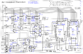
SRAM/EPROM Schematic

Software
The magazine article contains three listings with examples on how to use the Pseudo ROM board, including a ROM version of the Schneiderware Real Time Clock driver.
Scanned Article
- Schneiderware 8 - Pseudo ROM.pdf - SRAM and EPROM mapped as ROM - 4/1987 page 26-34, plus corrections in 5/1987 page 32-34