Difference between revisions of "8255"
(→PPI Control) |
(→PPI Port B) |
||
| (23 intermediate revisions by the same user not shown) | |||
| Line 1: | Line 1: | ||
== 8255 Part numbers used in the CPC during its lifetime == | == 8255 Part numbers used in the CPC during its lifetime == | ||
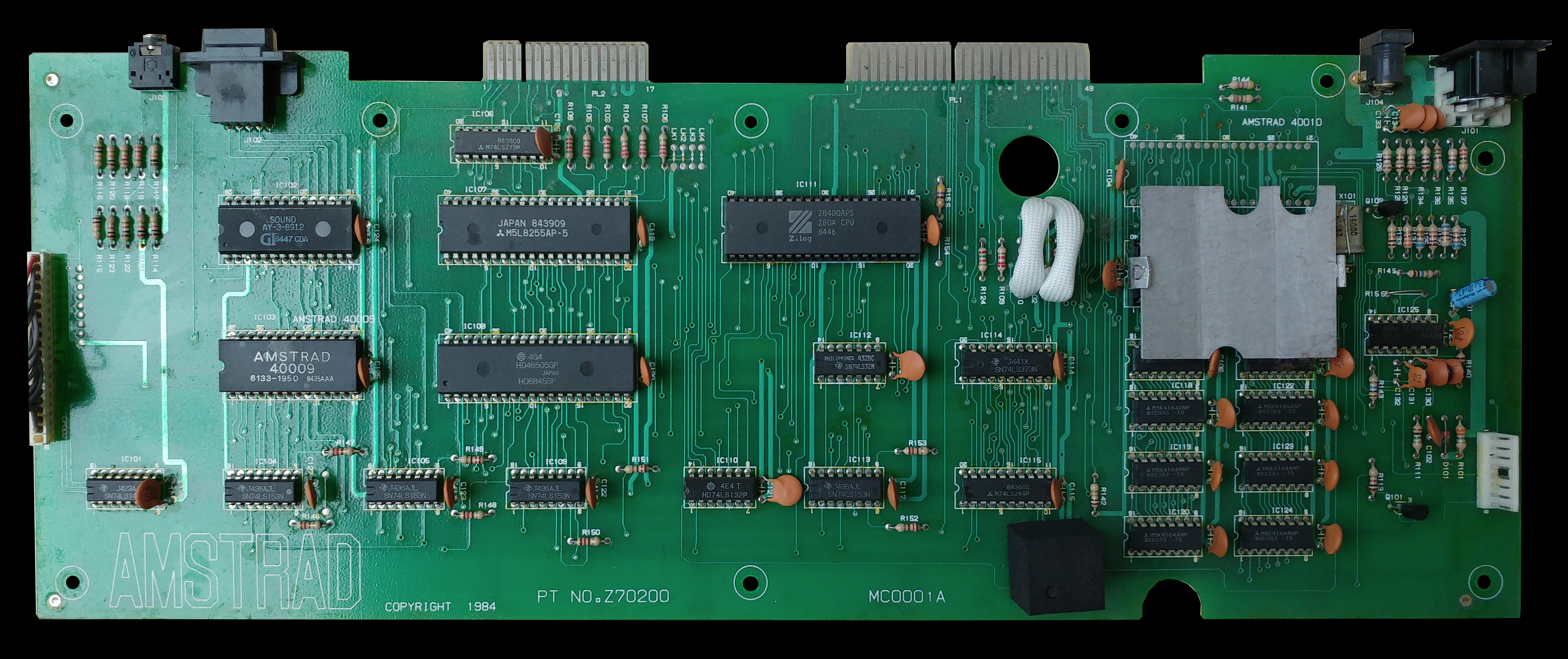
| − | * NEC D8255AC-2 | + | * Mitsubishi M5L8255AP-5 [https://www.cpcwiki.eu/imgs/8/80/MC0001A-v2-components.jpg Source] |
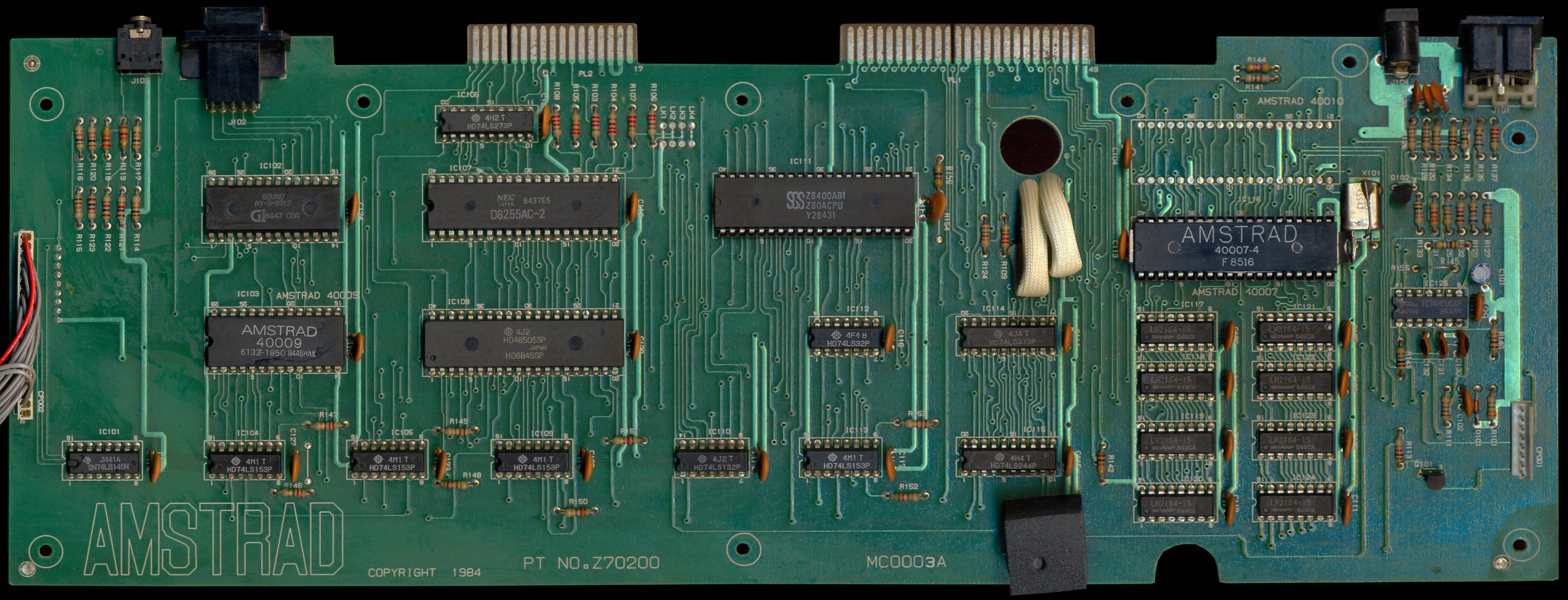
| − | * NEC D8255AC-5 | + | * NEC D8255AC-2 [https://www.cpcwiki.eu/imgs/d/da/Amstrad_CPC464_Z70200_MC0003A_PCB_Top.jpg Source] |
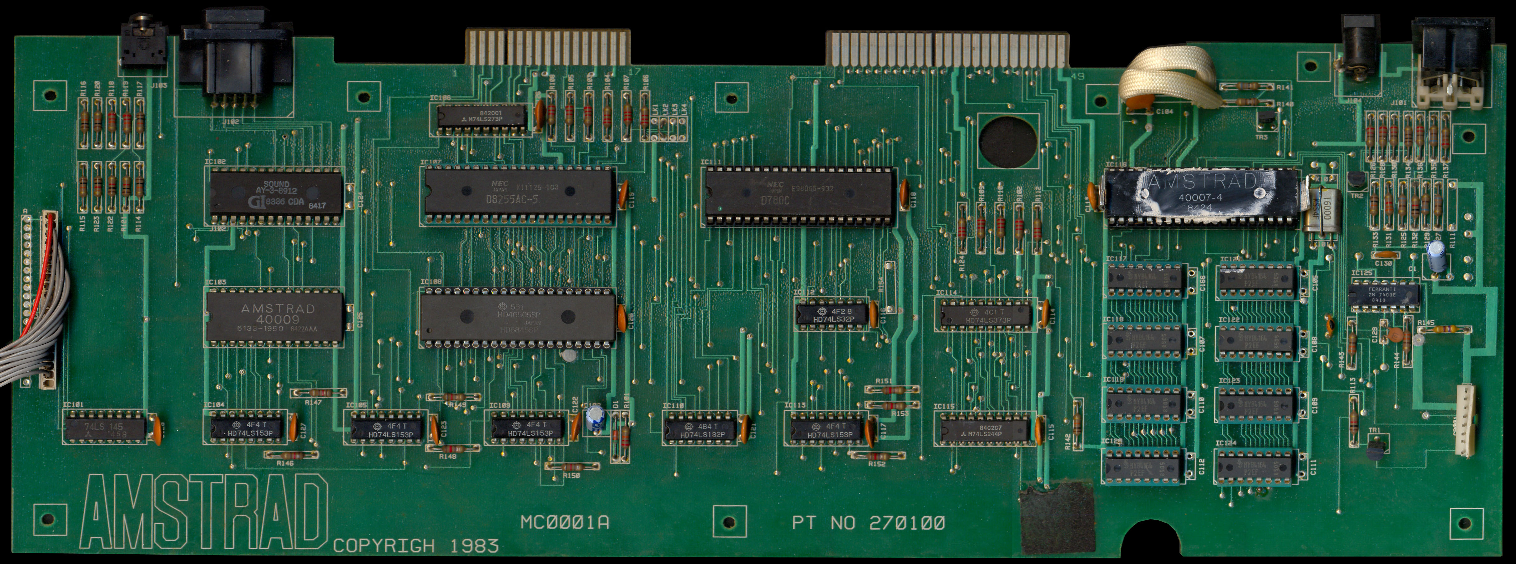
| − | * Toshiba TMP8255AP-5 | + | * NEC D8255AC-5 [https://www.cpcwiki.eu/imgs/c/c6/CPC464_270100_MC0001A_PCB_Top.jpg Source] |
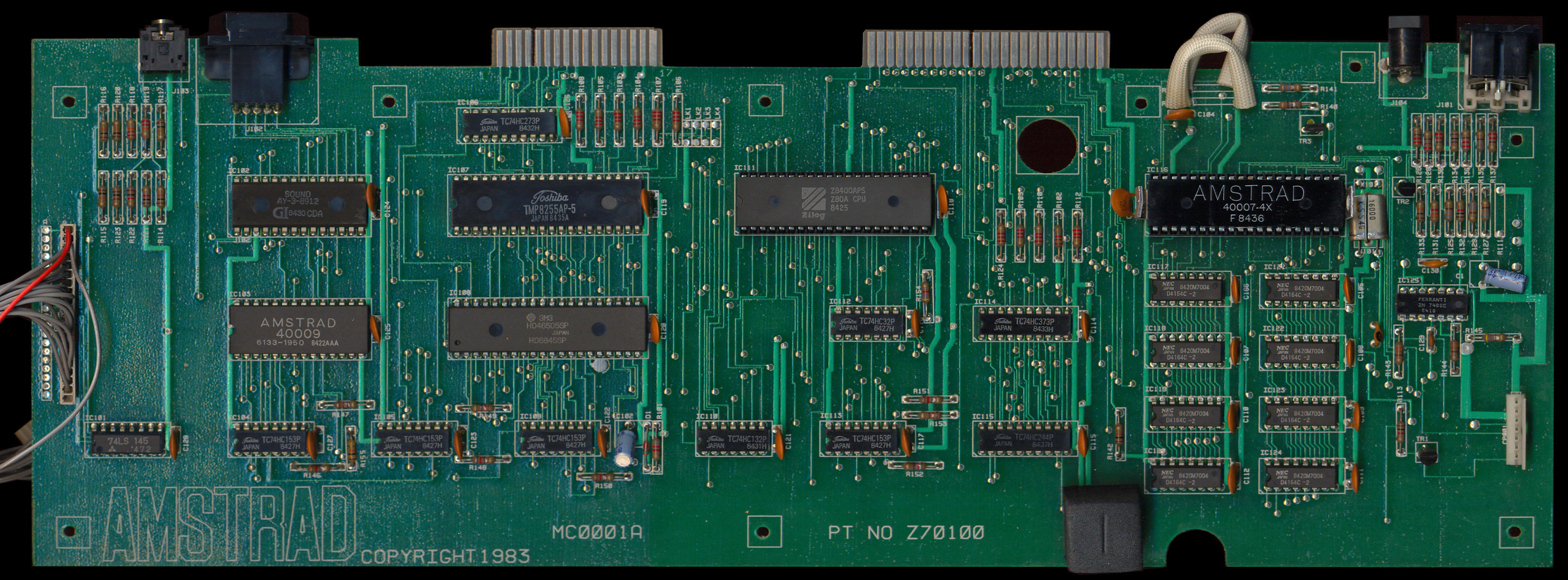
| + | * Toshiba TMP8255AP-5 [https://www.cpcwiki.eu/imgs/0/0d/CPC464_Z70100_MC0001A_PCB_Top.jpg Source] | ||
| − | All of these are almost identical in their operation. | + | All of these are almost identical in their operation. According to Kevin Thacker, it is possible to detect each version by writing and then reading from the ppi control i/o port. Each can give a different pattern of values that are read back. |
| + | |||
| + | The KP580BB55A is a Soviet clone of the Intel i8255. It is used in the [[KC Compact]] and the [[Aleste 520EX]] clones of the Amstrad CPC computer. | ||
<br> | <br> | ||
| Line 13: | Line 16: | ||
The [[8255 PPI chip]] is a general purpose input/output IC. This document will describe its role in the Amstrad CPC, CPC+ and KC compact systems. To understand its full functions please read the datasheet. | The [[8255 PPI chip]] is a general purpose input/output IC. This document will describe its role in the Amstrad CPC, CPC+ and KC compact systems. To understand its full functions please read the datasheet. | ||
| − | In these systems it is connected to the AY-3-8912 Programmable Sound Generator (PSG), keyboard, cassette recorder, the VSYNC of the 6845 CRTC and the "busy" signal from the parallel port. | + | In these systems it is connected to the [[PSG|AY-3-8912 Programmable Sound Generator (PSG)]], keyboard, cassette recorder, the VSYNC of the [[CRTC|6845 CRTC]] and the "busy" signal from the parallel port. |
The PPI is selected when A11 of the I/O port address is set to "0", A9 and A8 then define the PPI function access (as shown below), A15-A12 and A10 should be "1" (to prevent conflicts with other hardware), A7-A0 are don't care. So, resulting Port addresses are: | The PPI is selected when A11 of the I/O port address is set to "0", A9 and A8 then define the PPI function access (as shown below), A15-A12 and A10 should be "1" (to prevent conflicts with other hardware), A7-A0 are don't care. So, resulting Port addresses are: | ||
| − | {| | + | {| class="wikitable" |
| − | + | !I/O address | |
| + | !/CS (A11) | ||
| + | !A1 (A9) | ||
| + | !A0 (A8) | ||
| + | !Description | ||
| + | !Read/Write status | ||
| + | !Used Direction | ||
| + | !Used for | ||
|- | |- | ||
| − | |&F4xx||0||0||Port A Data||Read/Write||In/Out||[[PSG]] (Sound/Keyboard/Joystick) | + | |&F4xx||0||0||0||Port A Data||Read/Write||In/Out||[[PSG]] (Sound/Keyboard/Joystick) |
|- | |- | ||
| − | |&F5xx||0||1||Port B Data||Read/Write||In||Vsync/Jumpers/PrinterBusy/CasIn/Exp | + | |&F5xx||0||0||1||Port B Data||Read/Write||In||Vsync/Jumpers/PrinterBusy/CasIn/Exp |
|- | |- | ||
| − | |&F6xx||1||0||Port C Data||Read/Write||Out||KeybRow/CasOut/PSG | + | |&F6xx||0||1||0||Port C Data||Read/Write||Out||KeybRow/CasOut/PSG |
|- | |- | ||
| − | |&F7xx||1||1||Control||Write Only||Out||Control | + | |&F7xx||0||1||1||Control||Write Only||Out||Control |
|- | |- | ||
|} | |} | ||
| Line 49: | Line 59: | ||
* for reading data from PSG all bits must be set to input (thereafter, output direction should be restored, for compatibility with the BIOS). | * for reading data from PSG all bits must be set to input (thereafter, output direction should be restored, for compatibility with the BIOS). | ||
| − | {| | + | {| class="wikitable" |
| − | + | !Bit | |
| + | !Description | ||
| + | !Usage | ||
|- | |- | ||
|7-0||PSG.DATA||[[PSG]] Databus (Sound/Keyboard/Joystick) | |7-0||PSG.DATA||[[PSG]] Databus (Sound/Keyboard/Joystick) | ||
| Line 65: | Line 77: | ||
* Input | * Input | ||
| − | {| | + | {| class="wikitable" |
| − | + | !Bit | |
| + | !Description | ||
| + | !Usage in CPC | ||
| + | !Usage in [[KC Compact]] | ||
|- | |- | ||
|7||CAS.IN||Cassette data input||Same as on CPC | |7||CAS.IN||Cassette data input||Same as on CPC | ||
| Line 76: | Line 91: | ||
|4||LK4||Screen Refresh Rate ("1"=50Hz, "0"=60Hz)||Set to "1"=50Hz (but ignored by the KC BIOS, which always uses 50Hz even if LK4 is changed) | |4||LK4||Screen Refresh Rate ("1"=50Hz, "0"=60Hz)||Set to "1"=50Hz (but ignored by the KC BIOS, which always uses 50Hz even if LK4 is changed) | ||
|- | |- | ||
| − | |3||LK3|| rowspan="3" | | + | |3||LK3|| rowspan="3" |Distributor ID. Usually set to 4=[[Awa]], 5=[[Schneider]], or 7=[[Amstrad]] |
| + | See [[LK-selectable Brand Names]] for details | ||
| + | ||Purpose unknown (set to "1") | ||
|- | |- | ||
|2||LK2||Purpose unknown (set to "0") | |2||LK2||Purpose unknown (set to "0") | ||
| Line 84: | Line 101: | ||
|0||[[CRTC]] VSYNC||Vertical Sync ("1"=VSYNC active, "0"=VSYNC inactive)||Same as on CPC | |0||[[CRTC]] VSYNC||Vertical Sync ("1"=VSYNC active, "0"=VSYNC inactive)||Same as on CPC | ||
|- | |- | ||
| + | |} | ||
| + | |||
| + | {| class="wikitable" | ||
| + | |+ Distributor ID | ||
| + | !Bit 3 | ||
| + | !Bit 2 | ||
| + | !Bit 1 | ||
| + | !Brand name | ||
| + | |- | ||
| + | |0 | ||
| + | |0 | ||
| + | |0 | ||
| + | |Isp | ||
| + | |- | ||
| + | |0 | ||
| + | |0 | ||
| + | |1 | ||
| + | |Triumph | ||
| + | |- | ||
| + | |0 | ||
| + | |1 | ||
| + | |0 | ||
| + | |Saisho | ||
| + | |- | ||
| + | |0 | ||
| + | |1 | ||
| + | |1 | ||
| + | |Solavox | ||
| + | |- | ||
| + | |1 | ||
| + | |0 | ||
| + | |0 | ||
| + | |Awa | ||
| + | |- | ||
| + | |1 | ||
| + | |0 | ||
| + | |1 | ||
| + | |Schneider | ||
| + | |- | ||
| + | |1 | ||
| + | |1 | ||
| + | |0 | ||
| + | |Orion | ||
| + | |- | ||
| + | |1 | ||
| + | |1 | ||
| + | |1 | ||
| + | |Amstrad | ||
|} | |} | ||
| Line 103: | Line 168: | ||
* upper: output, lower: output | * upper: output, lower: output | ||
| − | {| | + | {| class="wikitable" |
| − | + | !Bit | |
| + | !Description | ||
| + | !Usage | ||
|- | |- | ||
| − | |7||PSG BDIR||PSG function selection | + | |7||PSG BDIR (Bus DIRection)||rowspan=2|PSG function selection |
|- | |- | ||
| − | |6||PSG BC1 | + | |6||PSG BC1 (Bus Control 1) |
|- | |- | ||
|5||Cassette Write data||Cassette Out (sometimes also used as Printer Bit7, see [[8bit Printer Ports]]) | |5||Cassette Write data||Cassette Out (sometimes also used as Printer Bit7, see [[8bit Printer Ports]]) | ||
| Line 115: | Line 182: | ||
|- | |- | ||
|3||rowspan=4|Keyboard line||rowspan=4|Select keyboard line to be scanned (0-15) | |3||rowspan=4|Keyboard line||rowspan=4|Select keyboard line to be scanned (0-15) | ||
| + | See [[Programming:Keyboard scanning]] for details | ||
|- | |- | ||
|2 | |2 | ||
| Line 124: | Line 192: | ||
|} | |} | ||
| − | PSG function selection | + | {| class="wikitable" |
| − | + | |+ [[PSG]] function selection | |
| − | + | !Bit 7 | |
| − | + | !Bit 6 | |
| + | !Function | ||
|- | |- | ||
|0||0||Inactive | |0||0||Inactive | ||
| Line 180: | Line 249: | ||
In some of these modes, port C is used as a control/status port for port A or B. It can be used to confirm when data transfer may take place, and reflect any other flags. The 8255 PPI is therefore supplied with the added option for the user to set or reset any individual bits in port C. | In some of these modes, port C is used as a control/status port for port A or B. It can be used to confirm when data transfer may take place, and reflect any other flags. The 8255 PPI is therefore supplied with the added option for the user to set or reset any individual bits in port C. | ||
| + | |||
| + | <br> | ||
=== Mode 0 – Simple Input/output mode === | === Mode 0 – Simple Input/output mode === | ||
| Line 185: | Line 256: | ||
[[File:8255 - mode-0.png]] | [[File:8255 - mode-0.png]] | ||
| + | |||
| + | <br> | ||
=== Mode 1 – Strobed Input/output or Handshake mode === | === Mode 1 – Strobed Input/output or Handshake mode === | ||
| Line 194: | Line 267: | ||
[[File:8255 - mode-1.png]] | [[File:8255 - mode-1.png]] | ||
| + | |||
| + | <br> | ||
=== Mode 2 – Bidirectional Mode === | === Mode 2 – Bidirectional Mode === | ||
| Line 199: | Line 274: | ||
[[File:8255 - mode-2.png]] | [[File:8255 - mode-2.png]] | ||
| + | |||
| + | <br> | ||
=== Port pins summary === | === Port pins summary === | ||
| Line 291: | Line 368: | ||
[[File:8255 Block Diagram.png]] | [[File:8255 Block Diagram.png]] | ||
| + | |||
| + | The PPI 8255 does not have a clock pin. It relies purely on control signals from the CPU to operate. It uses Read, Write, and Control signals to manage data transfers instead of a clock signal. This allows it to work effectively without needing its own clock input. | ||
<br> | <br> | ||
| Line 307: | Line 386: | ||
* [[Media:Intel8255A_datasheet.pdf]] PPI Datasheet (Intel) | * [[Media:Intel8255A_datasheet.pdf]] PPI Datasheet (Intel) | ||
* [[Media:PPI M5L8255AP-5.pdf]] PPI Datasheet (Mitsubishi) | * [[Media:PPI M5L8255AP-5.pdf]] PPI Datasheet (Mitsubishi) | ||
| + | * [[Media:Programmable Peripheral Interface TMP8255AP-5.pdf]] PPI Datasheet (Toshiba) | ||
* [https://github.com/jotego/jt8255 JT8255] Verilog implementation of the 8255 PPI | * [https://github.com/jotego/jt8255 JT8255] Verilog implementation of the 8255 PPI | ||
Latest revision as of 08:40, 30 March 2025
Contents
8255 Part numbers used in the CPC during its lifetime
All of these are almost identical in their operation. According to Kevin Thacker, it is possible to detect each version by writing and then reading from the ppi control i/o port. Each can give a different pattern of values that are read back.
The KP580BB55A is a Soviet clone of the Intel i8255. It is used in the KC Compact and the Aleste 520EX clones of the Amstrad CPC computer.
The 8255 in the CPC
The 8255 PPI chip is a general purpose input/output IC. This document will describe its role in the Amstrad CPC, CPC+ and KC compact systems. To understand its full functions please read the datasheet.
In these systems it is connected to the AY-3-8912 Programmable Sound Generator (PSG), keyboard, cassette recorder, the VSYNC of the 6845 CRTC and the "busy" signal from the parallel port.
The PPI is selected when A11 of the I/O port address is set to "0", A9 and A8 then define the PPI function access (as shown below), A15-A12 and A10 should be "1" (to prevent conflicts with other hardware), A7-A0 are don't care. So, resulting Port addresses are:
| I/O address | /CS (A11) | A1 (A9) | A0 (A8) | Description | Read/Write status | Used Direction | Used for |
|---|---|---|---|---|---|---|---|
| &F4xx | 0 | 0 | 0 | Port A Data | Read/Write | In/Out | PSG (Sound/Keyboard/Joystick) |
| &F5xx | 0 | 0 | 1 | Port B Data | Read/Write | In | Vsync/Jumpers/PrinterBusy/CasIn/Exp |
| &F6xx | 0 | 1 | 0 | Port C Data | Read/Write | Out | KeybRow/CasOut/PSG |
| &F7xx | 0 | 1 | 1 | Control | Write Only | Out | Control |
Group Mode 1 (Strobed Input/Output) and Group Mode 2 (Bi-Directional Bus), as far as I know, are not used by any program. Group Mode 0 (Basic Input/Output) is always used.
In the CPC+, the 8255 is integrated into the ASIC. The "emulation" is not complete and some functionality is not available. Please see the Extra CPC+ documentation for more information.
Port Usage
- NOTE - If you are using the firmware, always return the operating modes and I/O state of the ports used to their settings below. The firmware expects the settings to be the same as given below and may operate incorrectly if they are not.
PPI Port A
Operating system settings:
- I/O Mode 0,
- For writing data to PSG all bits must be set to output,
- for reading data from PSG all bits must be set to input (thereafter, output direction should be restored, for compatibility with the BIOS).
| Bit | Description | Usage |
|---|---|---|
| 7-0 | PSG.DATA | PSG Databus (Sound/Keyboard/Joystick) |
PPI Port B
Operating system settings:
- I/O Mode 0,
- Input
| Bit | Description | Usage in CPC | Usage in KC Compact |
|---|---|---|---|
| 7 | CAS.IN | Cassette data input | Same as on CPC |
| 6 | PRN.BUSY | Parallel/Printer port ready signal, "1" = not ready, "0" = Ready | Same as on CPC |
| 5 | /EXP | Expansion Port /EXP pin | Same as on CPC |
| 4 | LK4 | Screen Refresh Rate ("1"=50Hz, "0"=60Hz) | Set to "1"=50Hz (but ignored by the KC BIOS, which always uses 50Hz even if LK4 is changed) |
| 3 | LK3 | Distributor ID. Usually set to 4=Awa, 5=Schneider, or 7=Amstrad
See LK-selectable Brand Names for details |
Purpose unknown (set to "1") |
| 2 | LK2 | Purpose unknown (set to "0") | |
| 1 | LK1 | Expansion Port /TEST pin | |
| 0 | CRTC VSYNC | Vertical Sync ("1"=VSYNC active, "0"=VSYNC inactive) | Same as on CPC |
| Bit 3 | Bit 2 | Bit 1 | Brand name |
|---|---|---|---|
| 0 | 0 | 0 | Isp |
| 0 | 0 | 1 | Triumph |
| 0 | 1 | 0 | Saisho |
| 0 | 1 | 1 | Solavox |
| 1 | 0 | 0 | Awa |
| 1 | 0 | 1 | Schneider |
| 1 | 1 | 0 | Orion |
| 1 | 1 | 1 | Amstrad |
- LK1-4 are links on the mainboard ("0" bits are wired to GND). On CPC464,CPC664,CPC6128 and GX4000 they are labeled LK1-LK4, on the CPC464+ and CPC6128+ they are labeled LK101-LK103 (and LK104, presumably?).
- Bit5 (/EXP) can be used by a expansion device to report its presence. "1" = device connected, "0" = device not connected. This is not always used by all expansion devices. is it used by any expansions? [in the DDI-1 disc interface, /EXP connects to the ROM bank selection, bank 0 or bank 7]
- If port B is programmed as an output, you can make a fake vsync visible to the Gate-Array by writing 1 to bit 0. You can then turn it off by writing 0 to bit 0. It is fake in the sense that it is not generated by the CRTC as it normally is. This fake vsync doesn't work on all CPCs. It is not known if it is dependent on CRTC or 8255 or both.
- For more info on LK1-LK4 (and further LKs) see LK Links
PPI Port C
Operating system settings:
- upper: I/O Mode 0, lower: I/O mode 0,
- upper: output, lower: output
| Bit | Description | Usage |
|---|---|---|
| 7 | PSG BDIR (Bus DIRection) | PSG function selection |
| 6 | PSG BC1 (Bus Control 1) | |
| 5 | Cassette Write data | Cassette Out (sometimes also used as Printer Bit7, see 8bit Printer Ports) |
| 4 | Cassette Motor Control | set bit to "1" for motor on, or "0" for motor off |
| 3 | Keyboard line | Select keyboard line to be scanned (0-15)
See Programming:Keyboard scanning for details |
| 2 | ||
| 1 | ||
| 0 |
| Bit 7 | Bit 6 | Function |
|---|---|---|
| 0 | 0 | Inactive |
| 0 | 1 | Read from selected PSG register |
| 1 | 0 | Write to selected PSG register |
| 1 | 1 | Select PSG register |
PPI Control
This register has two different functions depending on bit7 of the data written to this register.
PPI Control with Bit7=0
If Bit 7 is "0" then the register is used to set or clear a single bit in Port C:
 Bit 0    B        New value for the specified bit (0=Clear, 1=Set)
 Bit 1-3  N0,N1,N2 Specifies the number of a bit (0-7) in Port C
 Bit 4-6  -        Not Used
 Bit 7    SF       Must be "0" in this case

PPI Control with Bit7=1
Otherwise, if Bit 7 is "1" then the other bits will initialize Group Modes and Ports A-B-Cupper-Clower as Input or Output:
 Bit 0    IO-Cl    Direction for Port C, lower bits (always 0=Output in CPC)
 Bit 1    IO-B     Direction for Port B             (always 1=Input in CPC)
 Bit 2    MS0      Mode for Port B and Port Cl      (always zero in CPC)
 Bit 3    IO-Ch    Direction for Port C, upper bits (always 0=Output in CPC)
 Bit 4    IO-A     Direction for Port A             (0=Output, 1=Input)
 Bit 5,6  MS0,MS1  Mode for Port A and Port Ch      (always zero in CPC)
 Bit 7    SF       Must be "1" to setup the above bits
- CAUTION: Writing to PIO Control Register (with Bit7 set), automatically resets PIO Ports A,B,C to 00h each!
- In the CPC only Bit 4 is of interest, all other bits are always having the same value. In order to write to the PSG sound registers, a value of 82h must be written to this register. In order to read from the keyboard (through PSG register 0Eh), a value of 92h must be written to this register.

Group Modes
In some of these modes, port C is used as a control/status port for port A or B. It can be used to confirm when data transfer may take place, and reflect any other flags. The 8255 PPI is therefore supplied with the added option for the user to set or reset any individual bits in port C.
Mode 0 – Simple Input/output mode
In this mode, the ports can be used for simple I/O operations without handshaking signals. Port A, port B provide simple I/O operation. The two halves of port C can be either used together as an additional 8-bit port, or they can be used as individual 4-bit ports. Since the two halves of port C are independent, they may be used such that one-half is initialized as an input port while the other half is initialized as an output port.

Mode 1 – Strobed Input/output or Handshake mode
When we wish to use port A or port B for handshake (strobed) input or output operation, we initialise that port in mode 1 (port A and port B can be initialised to operate in different modes, i.e., for e.g., port A can operate in mode 0 and port B in mode 1). Some of the pins of port C function as handshake lines.
For port B in this mode (irrespective of whether is acting as an input port or output port), PC0, PC1 and PC2 pins function as handshake lines.
If port A is initialised as mode 1 input port, then, PC3, PC4 and PC5 function as handshake signals. Pins PC6 and PC7 are available for use as input/output lines.

Mode 2 – Bidirectional Mode
Only port A can be initialized in this mode. Port A can be used for bidirectional handshake data transfer. This means that data can be input or output on the same eight lines (PA0 - PA7). Pins PC3 - PC7 are used as handshake lines for port A. The remaining pins of port C (PC0 - PC2) can be used as input/output lines if group B is initialized in mode 0 or as handshaking for port B if group B is initialized in mode 1. In this mode, the 8255 may be used to extend the system bus to a slave microprocessor or to transfer data bytes to and from a floppy disk controller. Acknowledgement and handshaking signals are provided to maintain proper data flow and synchronisation between the data transmitter and receiver.

Port pins summary

Programming Examples
1. Using the control byte
- Setting bit 7 of port C to 1,
            LD B,&F7                ;8255 Control port
            LD A,%00001111          ;Bit Set/reset function
            OUT (C),A               ;Send it to 8255
            RET
- Set port A to input, operating in mode 0, port B to output, operating in mode 0 and port C to input, operating in mode 0.
            LD B,&F7                ;8255 Control port
            LD A,%10011001          ;Configuration function
            OUT (C),A               ;Send it to 8255
            RET
2. Using port A/B/C,
In this example, port A is set to output, port B is set to input, and port C is set to output, and they are all operating in mode 0.
We will only be using port A for these examples.
- Reading from port A,
                                    ;Set port A to input

            LD B,&F7                ;8255 Control port
            LD A,%10010010          ;Configuration function
            OUT (C),A               ;Send to 8255

            LD B,&F4                ;Port A port address
            IN E,(C)                ;Get byte from port

                                    ;Register E holds value from port

                                    ;Return port I/O status and operating modes
                                    ;to previous settings.

            LD B,&F7                ;8255 Control port
            LD A,%10000010          ;Configuration function
            OUT (C),A               ;Send to 8255
            RET
- Writing to port A,
                                    ;Set port A to output

                                    ;(Note the next few lines are not necessary
                                    ;as port A is already acting as output, however
                                    ;it is given here just to make the example
                                    ;more understandable)

            LD B,&F7                ;8255 Control port
            LD A,%10000010          ;Configuration function
            OUT (C),A               ;Send to 8255

            LD B,&F4                ;port A port address

                                    ;Register E holds value to put into port

            LD E,&FF                ;Data to put into port
            OUT (C),E               ;Send to port A

                                    ;Return port I/O status and operating modes
                                    ;to previous settings.

            LD B,&F7                ;8255 Control port
            LD A,%10000010          ;Configuration function
            OUT (C),A
            RET
Block Diagram

The PPI 8255 does not have a clock pin. It relies purely on control signals from the CPU to operate. It uses Read, Write, and Control signals to manage data transfers instead of a clock signal. This allows it to work effectively without needing its own clock input.
Amstrad ASIC PPI
- The 8255 PPI is not emulated by the Pre-ASIC. These CPCs have a real PPI chip and therefore behave like the first generation of CPCs.
- The ASIC PPI does not support Group Modes other than Groupe Mode 0.
- On the ASIC PPI, Port B is always defined as input and Port C is always defined as output.
- On a real PPI chip, when the PPI control register is used (with bit7=1) to configure the ports, the output latches of all ports are reset to 0. The ASIC poorly emulates the PPI and does not reset these ports.
Resources
- Media:Intel8255A_datasheet.pdf PPI Datasheet (Intel)
- Media:PPI M5L8255AP-5.pdf PPI Datasheet (Mitsubishi)
- Media:Programmable Peripheral Interface TMP8255AP-5.pdf PPI Datasheet (Toshiba)
- JT8255 Verilog implementation of the 8255 PPI