
The Z80 is an 8-bit microprocessor designed by Zilog founder and CEO Federico Faggin. It is a successor of the Intel 8080, also designed by Federico Faggin. First released in July 1976, this CPU is used in the Amstrad CPC / Plus / PCW computers.
The Z80/Z80A was a very popular microprocessor, used in a wide range of applications, from gaming consoles like the ColecoVision, the Sega Master System and Sega GameGear to personal computers like the ZX81, ZX Spectrum and MSX.
It was used in the Commodore C128 as a secondary processor in order to achieve CP/M compatibility. Similarly, the Acorn Z80 Second Processor expansion for the BBC Micro enabled CP/M compatibility. And the popular Z-80 SoftCard expansion did the same for the Apple II.
The best-selling devices to feature a Zilog Z80 are the Sega MegaDrive with 40 million units sold Source, and the TI graphing calculators with 90 million units sold Source.
Although there were definitely other CPUs in use in the 1980s, the vast majority of microcomputers people had at home or at the office used either a MOS 6502 (or one of its variants), a Zilog Z80, an early member of the Intel 8086 family, or a Motorola 68000.
History
In the early 1970s, Intel developed the 8080, one of the first widely used microprocessors. However, a group of engineers led by Federico Faggin, the originator of the 8080 architecture in early 1972, left Intel to start their own company called Zilog in 1974.
At Zilog, Faggin and his team wanted to create an improved version of the Intel 8080 that would be more efficient, flexible, and easier to use. This led to the development of the Z80, which was designed to be both backward-compatible with the 8080 and more powerful. This compatibility meant that any software written for the 8080 could run on the Z80, making it an attractive upgrade for manufacturers and developers.
The Z80 had several key improvements over the 8080. It featured more registers, block instructions, bitwise ops, indexed addressing, and improved interrupt handling. It also had built-in memory refresh for dynamic RAM, that made it easier to build systems around it.
Description
The Z80 microprocessor is an 8-bit CPU with a 4-bit ALU and a 16-bit address bus capable of direct access to 64KB of memory space. The Z80 is a little-endian CPU, meaning it stores 16-bit values with the least significant byte first, followed by the most significant byte.
It has a language of 252 root instructions and with the reserved 4 bytes as prefixes, access to an additional 308 instructions. Although it lacks the raw processing power of processors like the Intel 80x86 or the Motorola 68000 series, the Z80 is extremely useful for low cost control applications.
The Z80 has about 8500 transistors. To put it into perspective, 64KB of DRAM contains 524288 transistors, as 1 bit of DRAM needs 1 transistor. Fun fact: an Amstrad CPC equipped with a 4MB RAM expansion has 32 million transistors dedicated to RAM while the Z80 CPU still has only 8500 transistors.
The Z80 is mid-1970s technology while the 64KB DRAM is early-1980s technology and the 4MB DRAM is early-1990s technology.
The Z80 comes in a 40-pin DIP package. It has been manufactured in A, B, and C models, differing only in maximum clock speed. It also has been manufactured as a stand-alone microcontroller with various configurations of on-chip RAM and EPROM.
Register File
| Register | Size | Description | Notes |
|---|---|---|---|
| B, C, D, E, H, L | 8-bit | General-purpose registers | Can form 16-bit pairs: BC, DE, HL |
| A (Accumulator) | 8-bit | Main register for arithmetic, logic, and data transfer | Most used register |
| F (Flags) | 8-bit |
|
Flags (including F5 and F3) are affected by most operations.
HF and NF are used in the DAA algorithm. |
| AF', BC', DE', HL' | 16-bit | Alternate register set | Swappable with primary registers for fast context switching |
| SP (Stack Pointer) | 16-bit | Points to top of the stack | Used for subroutine calls and interrupt handling |
| PC (Program Counter) | 16-bit | Points to the next instruction | Automatically increments as instructions execute |
| IX, IY (Index Registers) | 16-bit | Used for indexed addressing | Can be split into IXH/IXL, IYH/IYL for 8-bit access |
| I (Interrupt Vector) | 8-bit | Holds base address for interrupt mode 2 | Combined with external data to form an interrupt vector |
| R (Memory Refresh) | 8-bit | Increments after each M1 cycle (instruction or prefix fetch) to refresh DRAM | Only the lower 7 bits are incremented.
Bit7 can only be changed by writing to the R register. |
While the ALU is responsible for most flag changes, other instructions like stack operations (POP AF), specific register loads (LD A,I/R), direct flag commands (SCF, CCF), bit tests (BIT), and the control logic within block instructions also modify the flag register.
Internal State
| Register | Size | Description | Notes |
|---|---|---|---|
| IM (Interrupt Mode) | 2-bit | Specifies the interrupt mode (0, 1, or 2) | Controls how interrupts are handled:
The NMI vector is fixed at 0066h, regardless of the I register, and of the IM interrupt mode. |
| IFF1 | 1-bit | Main Interrupt Flip-Flop | Set when interrupts are enabled, cleared on disable.
When the CPU accepts a maskable interrupt, both IFF1 and IFF2 are automatically cleared, inhibiting further interrupts. |
| IFF2 | 1-bit | Stores the state of IFF1 during Non-Maskable Interrupts (NMI) | When an NMI occurs, the processor clears IFF1 to disable interrupts temporarily.
IFF2 stores the previous state of IFF1 so that after the NMI is handled, IFF1 can be restored to its original state. A barebone Amstrad CPC doesn't use NMI. So IFF1 and IFF2 are always the same. However, NMI is used by some expansions. |
| HALT | 1-bit | HALT state | /HALT indicates that the CPU has executed a HALT instruction and is waiting for either an NMI or an IRQ (with IFF1 enabled) before operation can resume.
Each cycle in the HALT state is a normal M1 (fetch) cycle except that the data received from the memory is ignored and an NOP instruction is forced internally to the CPU. The purpose of executing NOP instructions while in the HALT state is to keep the memory refresh signals active. |
| WZ | 16-bit | Internal temporary register pair. Also known as MEMPTR | Used for memory and address calculations.
Normally, you never see the content of this register. But it leaks through the flags F5 and F3 in the BIT b,(HL) instruction. Source |
| Q | 8-bit | Internal register where it assembles the new content of the F register, before moving it back to F |
 On Zilog NMOS Z80, when the instruction doesn't compute new flags, this register is cleared instead. But not on NEC NMOS Z80. And CMOS Z80 behave in a different way too.
 Normally, you never see the content of this register. But it leaks through F5 and F3 in the SCF/CCF instructions. Source
 Only 1 extra bit (F-changed) is needed for emulation Source. Also note that while POP AF and EX AF,AF' modify F, they do not compute new flag values. Source
The explanation above is just an approximation. In fact, SCF/CCF instructions are unstable. Source As of Oct 2024, this is now fully understood. Everything happens due to the fact that two internal buses HBUS and LBUS, to which the contents of registers A and F are issued at the beginning of the instruction, respectively, at some point are electrically combined. And in those bits where opposite values 0 and 1 are combined, a certain average potential appears, conditional 0.5. And then, these values are written back to the F register, and depending on the threshold of the transistor gates, these conditional 0.5 can turn into both 0 and 1. Source (RU) |
| IR (Instruction Register) | 8-bit | Holds the opcode of the currently executing instruction | Internally used, not accessible by the programmer. Not to be confused with I (Interrupt Vector) and R (Memory Refresh) registers. |
| EIP (Extended Instruction Prefix) | 2-bit | Holds the prefix for extended instructions (CB, ED, or none) | Used for extended instruction sets like bitwise ops. |
| IMP (Indexing Mode Prefix) | 2-bit | Specifies the indexing mode (DD for IX+d, FD for IY+d, or none for HL) | Indicates use of index registers (IX or IY) for memory access. |
Notes:
- EIP and IMP can be fusioned into a 3-bit internal state as there are only 7 possible values for the prefixes (none, ed, dd, fd, cb, ddcb, fdcb). Probably not a win though as it makes everything more confusing.
- IFF1 / IFF2 are called IEF1 / IEF2 (Interrupt Enable Flip-flops) in the Zilog eZ80 manual.
Addressing Modes
| Addressing Mode | Example | Operation |
|---|---|---|
| 8-bit Immediate | LD A, 5Ah | A ← 5Ah |
| 16-bit Immediate | LD HL, 1234h | HL ← 1234h |
| Register | LD A, B | A ← B |
| Register Indirect | LD A, (HL) | A ← M(HL) |
| Extended (Absolute) | LD A, (1234h) | A ← M(1234h) |
| Indexed (IX/IY+d) | LD A, (IX+5) | A ← M(IX+5) |
Many instructions, such as arithmetic instructions or loads, include more than one operand. In these cases, two different types of addressing can be employed in the same instruction.
For example, LD (HL),42 uses Immediate Addressing to specify the source and Register Indirect Addressing to specify the destination, to perform the operation: M(HL) ← 42.
Instruction Execution Sequence
For an instruction to fully execute, the Z80 goes through these key phases in order:
- Prefix and Opcode Fetch (M1)
- Operand Fetch (if needed)
- Memory Read / I/O Read (if needed)
- Operation
- Memory Write / I/O Write (if needed)
- At the end of every instruction, the IRQ (if IFF1 is active) and NMI pins are checked
- Loop (for block instructions only)
For example, the instruction RL (IX+42) will execute as follow:
- M1 (4 t-states): Prefix fetch &DD then increment PC
- M1 (4 t-states): Opcode fetch &CB (the second prefix) then increment PC
- M2 (3 t-states): Operand fetch 42 (the displacement byte) then increment PC
- M3 (5 t-states): Operand fetch &16 (the real opcode) then increment PC, while calculating the address IX+42
- M4 (4 t-states): Memory read at address IX+42 then RL operation
- M5 (3 t-states): Memory write at address IX+42
Z80 Instructions
Legend
| Notation | Meaning | Operand bits |
|---|---|---|
| d | 8-bit signed relative offset | dddddddd |
| e | 16-bit relative address | eeeeeeee |
| n | 8-bit immediate | nnnnnnnn |
| nn | 16-bit address or immediate | lolololo hihihihi |
Flags
- - = no change
- + = change by definition (if noted, by the operation marked with '=> flags', otherwise by the only non-single-bit operation):
* S = sign, bit 7 of the result byte (accumulator or high byte for 16-bit operations)
* Z = zero, set if the result is zero (8 or 16-bit value)
* 5 = undocumented, bit 5 of the result byte
* H = half-carry, the carry (theoretical bit 4) of the low nibble of the result byte
* 3 = undocumented, bit 3 of the result byte
* P = parity (set if the result byte has an even number of bits set) or overflow (set when crossing the boundary of the signed range); always specified
* N = negative, set if the previous operation was a subtraction; always specified
* C = carry, the theoretical bit 8 of the result byte
- 0 = always reset
- 1 = always set
- X = change described under effect
- P = parity (only for the parity flag)
- V = overflow (only for the parity flag)
- A = OR with the respective bit of the accumulator
- C = set if the counter (bc) is nonzero after decrementing
Registers
- r,r̃: 000=B, 001=C, 010=D, 011=E, 100=H, 101=L, 111=A (110 is treated separately)
- s,s̃: 000=B, 001=C, 010=D, 011=E, 100=IXH/IYH, 101=IXL/IYL, 111=A (110 is treated separately)
- pp: 00=BC, 01=DE, 10=HL, 11=SP
- p̃p̃: 00=BC, 01=DE, 10=HL, 11=AF
- qq: 00=BC, 01=DE, 10=IX/IY, 11=SP
- q̃q̃: 00=BC, 01=DE, 10=IX/IY, 11=AF
Miscellaneous
- () = indirection
- (()) = I/O port
- [] = operator precedence (to avoid confusion with indirection)
- e.b = the bth bit of the value of expression e
- * = any bit value (0 or 1)
- wz = an internal 16-bit register connected to 16-bit operations
- tmp, tmp2 = temporary storage whose value is thrown away after each instruction
M-Cycle Sequences have been deduced logically and verified on real hardware. See Arduino Z80 dongle bus activity dump.
Load group
| Instruction | Opcode | Hexcode | NOPs | Cycles | M-Cycle Sequence | S | Z | 5 | H | 3 | P | N | C | Effect | Description |
|---|---|---|---|---|---|---|---|---|---|---|---|---|---|---|---|
| ld r,r̃ | 01rrrr̃r̃r̃ | 40-6F/78-7F | 1 | 4 (4) | M1 | - | - | - | - | - | - | - | - | r := r̃ | 8-bit Load |
| ld (hl),r | 01110rrr | 70-75/77 | 2 | 7 (4,3) | M1, MW | (hl) := r | |||||||||
| ld r,(hl) | 01rrr110 | 46/4E/56/5E/66/6E/7E | 2 | 7 (4,3) | M1, MR | r := (hl) | |||||||||
| ld s,s̃ | 01ssss̃s̃s̃ | DD/FD 40-6F/78-7F | 2 | 8 (4,4) | M1, M1 | s := s̃ | |||||||||
| ld (ixy+d),r | 01110rrr | DD/FD 70-75/77 dd | 5 | 19 (4,4,3,5,3) | M1, M1, MRd, INT(5), MW | (ixy+d) := r | |||||||||
| ld r,(ixy+d) | 01rrr110 | DD/FD 46/4E/56/5E/66/6E/7E dd | 5 | 19 (4,4,3,5,3) | M1, M1, MRd, INT(5), MR | r := (ixy+d) | |||||||||
| ld r,n | 00rrr110 | 06/0E/16/1E/26/2E/3E nn | 2 | 7 (4,3) | M1, MRn | r := n | |||||||||
| ld (hl),n | 00110110 | 36 nn | 3 | 10 (4,3,3) | M1, MRn, MW | (hl) := n | |||||||||
| ld (ixy+d),n | 00110110 | DD/FD 36 dd nn | 6 | 19 (4,4,3,5,3) | M1, M1, MRd, MRn, INT(2), MW | (ixy+d) := n | |||||||||
| ld (bc),a | 00000010 | 02 | 2 | 7 (4,3) | M1, MW | (bc) := a | |||||||||
| ld a,(bc) | 00001010 | 0A | 2 | 7 (4,3) | M1, MR | a := (bc) | |||||||||
| ld (de),a | 00010010 | 12 | 2 | 7 (4,3) | M1, MW | (de) := a | |||||||||
| ld a,(de) | 00011010 | 1A | 2 | 7 (4,3) | M1, MR | a := (de) | |||||||||
| ld (nn),a | 00110010 | 32 lo hi | 4 | 13 (4,3,3,3) | M1, MRl, MRh, MW | (nn) := a | |||||||||
| ld a,(nn) | 00111010 | 3A lo hi | 4 | 13 (4,3,3,3) | M1, MRl, MRh, MR | a := (nn) | |||||||||
| ld pp,nn | 00pp0001 | 01/11/21/31 lo hi | 3 | 10 (4,3,3) | M1, MRl, MRh | - | - | - | - | - | - | - | - | pp := nn | 16-bit Load |
| ld qq,nn | 00qq0001 | DD/FD 01/11/21/31 lo hi | 4 | 14 (4,4,3,3) | M1, M1, MRl, MRh | qq := nn | |||||||||
| ld (nn),hl | 00100010 | 22 lo hi | 5 | 16 (4,3,3,3,3) | M1, MRl, MRh, MW, MW | (nn) := hl | |||||||||
| ld (nn),ixy | 00100010 | DD/FD 22 lo hi | 6 | 20 (4,4,3,3,3,3) | M1, M1, MRl, MRh, MW, MW | (nn) := ixy | |||||||||
| ld (nn),pp | 01pp0011 | ED 43/53/63/73 lo hi | 6 | 20 (4,4,3,3,3,3) | M1, M1, MRl, MRh, MW, MW | (nn) := pp | |||||||||
| ld hl,(nn) | 00101010 | 2A lo hi | 5 | 16 (4,3,3,3,3) | M1, MRl, MRh, MR, MR | hl := (nn) | |||||||||
| ld ixy,(nn) | 00101010 | DD/FD 2A lo hi | 6 | 20 (4,4,3,3,3,3) | M1, M1, MRl, MRh, MR, MR | ixy := (nn) | |||||||||
| ld pp,(nn) | 01pp1011 | ED 4B/5B/6B/7B lo hi | 6 | 20 (4,4,3,3,3,3) | M1, M1, MRl, MRh, MR, MR | pp := (nn) | |||||||||
| ld sp,hl | 11111001 | F9 | 2 | 6 (6) | M1, INT(2) | sp := hl | |||||||||
| ld sp,ixy | 11111001 | DD/FD F9 | 3 | 10 (4,6) | M1, M1, INT(2) | sp := ixy | |||||||||
| pop p̃p̃ | 11p̃p̃0001 | C1/D1/E1/F1 | 3 | 10 (4,3,3) | M1, MR, MR | - | - | - | - | - | - | - | - | p̃p̃ := (sp), sp += 2 | Pop a value from the stack |
| pop q̃q̃ | 11q̃q̃0001 | DD/FD C1/D1/E1/F1 | 4 | 14 (4,4,3,3) | M1, M1, MR, MR | q̃q̃ := (sp), sp += 2 | |||||||||
| push p̃p̃ | 11p̃p̃0101 | C5/D5/E5/F5 | 4 | 11 (5,3,3) | M1, INT(1), MW, MW | - | - | - | - | - | - | - | - | sp -= 2, (sp) := p̃p̃ | Push a value onto the stack |
| push q̃q̃ | 11p̃p̃0101 | DD/FD C5/D5/E5/F5 | 5 | 15 (4,5,3,3) | M1, M1, INT(1), MW, MW | sp -= 2, (sp) := q̃q̃ |
16-bit Arithmetic group
| Instruction | Opcode | Hexcode | NOPs | Cycles | M-Cycle Sequence | S | Z | 5 | H | 3 | P | N | C | Effect | Description |
|---|---|---|---|---|---|---|---|---|---|---|---|---|---|---|---|
| inc pp | 00pp0011 | 03/13/23/33 | 2 | 6 (6) | M1, INT(2) | - | - | - | - | - | - | - | - | pp += 1 | Increment |
| inc qq | 00qq0011 | DD/FD 03/13/23/33 | 3 | 10 (4,6) | M1, M1, INT(2) | qq += 1 | |||||||||
| dec pp | 00pp1011 | 0B/1B/2B/3B | 2 | 6 (6) | M1, INT(2) | - | - | - | - | - | - | - | - | pp -= 1 | Decrement |
| dec qq | 00qq1011 | DD/FD 0B/1B/2B/3B | 3 | 10 (4,6) | M1, M1, INT(2) | qq -= 1 | |||||||||
| add hl,pp | 00pp1001 | 09/19/29/39 | 3 | 11 (4,4,3) | M1, INT(4), INT(3) | - | - | + | + | + | - | 0 | + | hl += pp | Add |
| add ixy,qq | 00qq1001 | DD/FD 09/19/29/39 | 4 | 15 (4,4,4,3) | M1, M1, INT(4), INT(3) | ixy += qq | |||||||||
| adc hl,qq | 01qq1010 | ED 4A/5A/6A/7A | 4 | 15 (4,4,4,3) | M1, M1, INT(4), INT(3) | + | + | + | + | + | V | 0 | + | hl += qq + cf | Add with Carry |
| sbc hl,qq | 01qq0010 | ED 42/52/62/72 | 4 | 15 (4,4,4,3) | M1, M1, INT(4), INT(3) | + | + | + | + | + | V | 1 | + | hl -= qq + cf | Subtract with Carry |
8-bit ALU group
| Instruction | Opcode | Hexcode | NOPs | Cycles | M-Cycle Sequence | S | Z | 5 | H | 3 | P | N | C | Effect | Description |
|---|---|---|---|---|---|---|---|---|---|---|---|---|---|---|---|
| inc r | 00rrr100 | 04/0C/14/1C/24/2C/3C | 1 | 4 (4) | M1 | + | + | + | + | + | V | 0 | - | r += 1 | Increment |
| inc s | 00sss100 | DD/FD 04/0C/14/1C/24/2C/3C | 2 | 8 (4,4) | M1, M1 | s += 1 | |||||||||
| inc (hl) | 00110100 | 34 | 3 | 11 (4,4,3) | M1, MR, INT(1), MW | (hl) += 1 | |||||||||
| inc (ixy+d) | 00110100 | DD/FD 34 dd | 6 | 23 (4,4,3,5,4,3) | M1, M1, MRd, INT(5), MR, INT(1), MW | (ixy+d) += 1 | |||||||||
| dec r | 00rrr101 | 05/0D/15/1D/25/2D/3D | 1 | 4 (4) | M1 | + | + | + | + | + | V | 1 | - | r -= 1 | Decrement |
| dec s | 00sss101 | DD/FD 05/0D/15/1D/25/2D/3D | 2 | 8 (4,4) | M1, M1 | s -= 1 | |||||||||
| dec (hl) | 00110101 | 35 | 3 | 11 (4,4,3) | M1, MR, INT(1), MW | (hl) -= 1 | |||||||||
| dec (ixy+d) | 00110101 | DD/FD 35 dd | 6 | 23 (4,4,3,5,4,3) | M1, M1, MRd, INT(5), MR, INT(1), MW | (ixy+d) -= 1 | |||||||||
| add a,n | 11000110 | C6 nn | 2 | 7 (4,3) | M1, MRn | + | + | + | + | + | V | 0 | + | a += n | Add |
| add a,r | 10000rrr | 80-85/87 | 1 | 4 (4) | M1 | a += r | |||||||||
| add a,s | 10000sss | DD/FD 80-85/87 | 2 | 8 (4,4) | M1, M1 | a += s | |||||||||
| add a,(hl) | 10000110 | 86 | 2 | 7 (4,3) | M1, MR | a += (hl) | |||||||||
| add a,(ixy+d) | 10000110 | DD/FD 86 dd | 5 | 19 (4,4,3,5,3) | M1, M1, MRd, INT(5), MR | a += (ixy+d) | |||||||||
| adc a,n | 11001110 | CE nn | 2 | 7 (4,3) | M1, MRn | + | + | + | + | + | V | 0 | + | a += n + cf | Add with Carry |
| adc a,r | 10001rrr | 88-8D/8F | 1 | 4 (4) | M1 | a += r + cf | |||||||||
| adc a,s | 10001sss | DD/FD 88-8D/8F | 2 | 8 (4,4) | M1, M1 | a += s + cf | |||||||||
| adc a,(hl) | 10001110 | 8E | 2 | 7 (4,3) | M1, MR | a += (hl) + cf | |||||||||
| adc a,(ixy+d) | 10001110 | DD/FD 8E dd | 5 | 19 (4,4,3,5,3) | M1, M1, MRd, INT(5), MR | a += (ixy+d) + cf | |||||||||
| sub n | 11010110 | D6 nn | 2 | 7 (4,3) | M1, MRn | + | + | + | + | + | V | 1 | + | a -= n | Subtract |
| sub r | 10010rrr | 90-95/97 | 1 | 4 (4) | M1 | a -= r | |||||||||
| sub s | 10010sss | DD/FD 90-95/97 | 2 | 8 (4,4) | M1, M1 | a -= s | |||||||||
| sub (hl) | 10010110 | 96 | 2 | 7 (4,3) | M1, MR | a -= (hl) | |||||||||
| sub (ixy+d) | 10010110 | DD/FD 96 dd | 5 | 19 (4,4,3,5,3) | M1, M1, MRd, INT(5), MR | a -= (ixy+d) | |||||||||
| sbc a,n | 11011110 | DE nn | 2 | 7 (4,3) | M1, MRn | + | + | + | + | + | V | 1 | + | a -= n + cf | Subtract with Carry |
| sbc a,r | 10011rrr | 98-9D/9F | 1 | 4 (4) | M1 | a -= r + cf | |||||||||
| sbc a,s | 10011sss | DD/FD 98-9D/9F | 2 | 8 (4,4) | M1, M1 | a -= s + cf | |||||||||
| sbc a,(hl) | 10011110 | 9E | 2 | 7 (4,3) | M1, MR | a -= (hl) + cf | |||||||||
| sbc a,(ixy+d) | 10011110 | DD/FD 9E dd | 5 | 19 (4,4,3,5,3) | M1, M1, MRd, INT(5), MR | a -= (ixy+d) + cf | |||||||||
| cp n | 11111110 | FE nn | 2 | 7 (4,3) | M1, MRn | + | + | X | + | X | V | 1 | + | tmp := a - n, f5 := n.5, f3 := n.3 | Compare |
| cp r | 10111rrr | B8-BD/BF | 1 | 4 (4) | M1 | tmp := a - r, f5 := r.5, f3 := r.3 | |||||||||
| cp s | 10111sss | DD/FD B8-BD/BF | 2 | 8 (4,4) | M1, M1 | tmp := a - s, f5 := s.5, f3 := s.3 | |||||||||
| cp (hl) | 10111110 | BE | 2 | 7 (4,3) | M1, MR | tmp := a - (hl), f5 := (hl).5, f3 := (hl).3 | |||||||||
| cp (ixy+d) | 10111110 | DD/FD BE dd | 5 | 19 (4,4,3,5,3) | M1, M1, MRd, INT(5), MR | tmp := a - (ixy+d), f5 := (ixy+d).5, f3 := (ixy+d).3 | |||||||||
| and n | 11100110 | E6 nn | 2 | 7 (4,3) | M1, MRn | + | + | + | 1 | + | P | 0 | 0 | a := a and n | Logical AND |
| and r | 10100rrr | A0-A5/A7 | 1 | 4 (4) | M1 | a := a and r | |||||||||
| and s | 10100sss | DD/FD A0-A5/A7 | 2 | 8 (4,4) | M1, M1 | a := a and s | |||||||||
| and (hl) | 10100110 | A6 | 2 | 7 (4,3) | M1, MR | a := a and (hl) | |||||||||
| and (ixy+d) | 10100110 | DD/FD A6 dd | 5 | 19 (4,4,3,5,3) | M1, M1, MRd, INT(5), MR | a := a and (ixy+d) | |||||||||
| xor n | 11101110 | EE nn | 2 | 7 (4,3) | M1, MRn | + | + | + | 0 | + | P | 0 | 0 | a := a xor n | Logical eXclusive OR |
| xor r | 10101rrr | A8-AD/AF | 1 | 4 (4) | M1 | a := a xor r | |||||||||
| xor s | 10101sss | DD/FD A8-AD/AF | 2 | 8 (4,4) | M1, M1 | a := a xor s | |||||||||
| xor (hl) | 10101110 | AE | 2 | 7 (4,3) | M1, MR | a := a xor (hl) | |||||||||
| xor (ixy+d) | 10101110 | DD/FD AE dd | 5 | 19 (4,4,3,5,3) | M1, M1, MRd, INT(5), MR | a := a xor (ixy+d) | |||||||||
| or n | 11110110 | F6 nn | 2 | 7 (4,3) | M1, MRn | + | + | + | 0 | + | P | 0 | 0 | a := a or n | Logical Inclusive OR |
| or r | 10110rrr | B0-B5/B7 | 1 | 4 (4) | M1 | a := a or r | |||||||||
| or s | 10110sss | DD/FD B0-B5/B7 | 2 | 8 (4,4) | M1, M1 | a := a or s | |||||||||
| or (hl) | 10110110 | B6 | 2 | 7 (4,3) | M1, MR | a := a or (hl) | |||||||||
| or (ixy+d) | 10110110 | DD/FD B6 dd | 5 | 19 (4,4,3,5,3) | M1, M1, MRd, INT(5), MR | a := a or (ixy+d) |
Note: Arithmetic operations ADD, ADC, SUB, SBC, CP calculate flags in the same way. Logic operations AND, XOR, OR calculate flags in the same way.
Note2: INC/DEC are meant to be used for loops and counters. They don't modify CF, to allow loops and counters to increment/decrement without disturbing carry-sensitive logic.
BCD group
| Instruction | Opcode | Hexcode | NOPs | Cycles | M-Cycle Sequence | S | Z | 5 | H | 3 | P | N | C | Effect | Description |
|---|---|---|---|---|---|---|---|---|---|---|---|---|---|---|---|
| daa | 00100111 | 27 | 1 | 4 (4) | M1 | + | + | + | X | + | P | - | X | tmp := a,
if nf then if hf or [a and 0x0f > 9] then tmp -= 0x06 if cf or [a > 0x99] then tmp -= 0x60 else if hf or [a and 0x0f > 9] then tmp += 0x06 if cf or [a > 0x99] then tmp += 0x60 endif, tmp => flags, cf := cf or [a > 0x99], hf := a.4 xor tmp.4, a := tmp |
Decimal Adjust Accumulator |
| rrd | 01100111 | ED 67 | 5 | 18 (4,4,3,4,3) | M1, M1, MR, INT(4), MW | + | + | + | 0 | + | P | 0 | - | tmp := (hl), (hl) := [tmp >> 4] + [[a and 0x0f] << 4],
a := [a and 0xf0] + [tmp and 0x0f] => flags |
Rotate Right Decimal |
| rld | 01101111 | ED 6F | 5 | 18 (4,4,3,4,3) | M1, M1, MR, INT(4), MW | + | + | + | 0 | + | P | 0 | - | tmp := [(hl) << 4] + [a and 0x0f], (hl) := tmp,
a := [a and 0xf0] + [tmp >> 8] => flags |
Rotate Left Decimal |
ROT group
| Instruction | Opcode | Hexcode | NOPs | Cycles | M-Cycle Sequence | S | Z | 5 | H | 3 | P | N | C | Effect | Description |
|---|---|---|---|---|---|---|---|---|---|---|---|---|---|---|---|
| rlca | 00000111 | 07 | 1 | 4 (4) | M1 | - | - | + | 0 | + | - | 0 | X | cf := a.7, a := [a << 1] + cf | Fast Rotate |
| rrca | 00001111 | 0F | 1 | 4 (4) | M1 | cf := a.0, a := [a >> 1] + [cf << 7] | |||||||||
| rla | 00010111 | 17 | 1 | 4 (4) | M1 | ocf := cf, cf := a.7, a := [a << 1] + ocf | |||||||||
| rra | 00011111 | 1F | 1 | 4 (4) | M1 | ocf := cf, cf := a.0, a := [a >> 1] + [ocf << 7] | |||||||||
| rlc r | 00000rrr | CB 00-05/07 | 2 | 8 (4,4) | M1, M1 | + | + | + | 0 | + | P | 0 | X | cf := r.7, r := [r << 1] + cf | Rotate Left Carry |
| rlc (ixy+d)->r | 00000rrr | DD/FD CB dd 00-05/07 | 7 | 23 (4,4,3,5,4,3) | M1, M1, MRd, MRo, INT(2), MR, INT(1), MW | cf := (ixy+d).7, (ixy+d) := r := [(ixy+d) << 1] + cf | |||||||||
| rlc (hl) | 00000110 | CB 06 | 4 | 15 (4,4,4,3) | M1, M1, MR, INT(1), MW | cf := (hl).7, (hl) := [(hl) << 1] + cf | |||||||||
| rlc (ixy+d) | 00000110 | DD/FD CB dd 06 | 7 | 23 (4,4,3,5,4,3) | M1, M1, MRd, MRo, INT(2), MR, INT(1), MW | cf := (ixy+d).7, (ixy+d) := [(ixy+d) << 1] + cf | |||||||||
| rrc r | 00001rrr | CB 08-0D/0F | 2 | 8 (4,4) | M1, M1 | + | + | + | 0 | + | P | 0 | X | cf := r.0, r := [r >> 1] + [cf << 7] | Rotate Right Carry |
| rrc (ixy+d)->r | 00001rrr | DD/FD CB dd 08-0D/0F | 7 | 23 (4,4,3,5,4,3) | M1, M1, MRd, MRo, INT(2), MR, INT(1), MW | cf := (ixy+d).0, (ixy+d) := r := [(ixy+d) >> 1] + [cf << 7] | |||||||||
| rrc (hl) | 00001110 | CB 0E | 4 | 15 (4,4,4,3) | M1, M1, MR, INT(1), MW | cf := (hl).0, (hl) := [(hl) >> 1] + [cf << 7] | |||||||||
| rrc (ixy+d) | 00001110 | DD/FD CB dd 0E | 7 | 23 (4,4,3,5,4,3) | M1, M1, MRd, MRo, INT(2), MR, INT(1), MW | cf := (ixy+d).0, (ixy+d) := [(ixy+d) >> 1] + [cf << 7] | |||||||||
| rl r | 00010rrr | CB 10-15/17 | 2 | 8 (4,4) | M1, M1 | + | + | + | 0 | + | P | 0 | X | ocf := cf, cf := r.7, r := [r << 1] + ocf | Rotate Left |
| rl (ixy+d)->r | 00010rrr | DD/FD CB dd 10-15/17 | 7 | 23 (4,4,3,5,4,3) | M1, M1, MRd, MRo, INT(2), MR, INT(1), MW | ocf := cf, cf := (ixy+d).7, (ixy+d) := r := [(ixy+d) << 1] + ocf | |||||||||
| rl (hl) | 00010110 | CB 16 | 4 | 15 (4,4,4,3) | M1, M1, MR, INT(1), MW | ocf := cf, cf := (hl).7, (hl) := [(hl) << 1] + ocf | |||||||||
| rl (ixy+d) | 00010110 | DD/FD CB dd 16 | 7 | 23 (4,4,3,5,4,3) | M1, M1, MRd, MRo, INT(2), MR, INT(1), MW | ocf := cf, cf := (ixy+d).7, (ixy+d) := [(ixy+d) << 1] + ocf | |||||||||
| rr r | 00011rrr | CB 18-1D/1F | 2 | 8 (4,4) | M1, M1 | + | + | + | 0 | + | P | 0 | X | ocf := cf, cf := r.0, r := [r >> 1] + [ocf << 7] | Rotate Right |
| rr (ixy+d)->r | 00011rrr | DD/FD CB dd 18-1D/1F | 7 | 23 (4,4,3,5,4,3) | M1, M1, MRd, MRo, INT(2), MR, INT(1), MW | ocf := cf, cf := (ixy+d).0, (ixy+d) := r := [(ixy+d) >> 1] + [ocf << 7] | |||||||||
| rr (hl) | 00011110 | CB 1E | 4 | 15 (4,4,4,3) | M1, M1, MR, INT(1), MW | ocf := cf, cf := (hl).0, (hl) := [(hl) >> 1] + [ocf << 7] | |||||||||
| rr (ixy+d) | 00011110 | DD/FD CB dd 1E | 7 | 23 (4,4,3,5,4,3) | M1, M1, MRd, MRo, INT(2), MR, INT(1), MW | ocf := cf, cf := (ixy+d).0, (ixy+d) := [(ixy+d) >> 1] + [ocf << 7] | |||||||||
| sla r | 00100rrr | CB 20-25/27 | 2 | 8 (4,4) | M1, M1 | + | + | + | 0 | + | P | 0 | X | cf := r.7, r := r << 1 | Shift Left Arithmetic |
| sla (ixy+d)->r | 00100rrr | DD/FD CB dd 20-25/27 | 7 | 23 (4,4,3,5,4,3) | M1, M1, MRd, MRo, INT(2), MR, INT(1), MW | cf := (ixy+d).7, (ixy+d) := r := (ixy+d) << 1 | |||||||||
| sla (hl) | 00100110 | CB 26 | 4 | 15 (4,4,4,3) | M1, M1, MR, INT(1), MW | cf := (hl).7, (hl) := (hl) << 1 | |||||||||
| sla (ixy+d) | 00100110 | DD/FD CB dd 26 | 7 | 23 (4,4,3,5,4,3) | M1, M1, MRd, MRo, INT(2), MR, INT(1), MW | cf := (ixy+d).7, (ixy+d) := (ixy+d) << 1 | |||||||||
| sra r | 00101rrr | CB 28-2D/2F | 2 | 8 (4,4) | M1, M1 | + | + | + | 0 | + | P | 0 | X | cf := r.0, r := r >> 1, r.7 := r.6 | Shift Right Arithmetic |
| sra (ixy+d)->r | 00101rrr | DD/FD CB dd 28-2D/2F | 7 | 23 (4,4,3,5,4,3) | M1, M1, MRd, MRo, INT(2), MR, INT(1), MW | cf := (ixy+d).0, tmp := (ixy+d) >> 1, tmp.7 := tmp.6, (ixy+d) := r := tmp | |||||||||
| sra (hl) | 00101110 | CB 2E | 4 | 15 (4,4,4,3) | M1, M1, MR, INT(1), MW | cf := (hl).0, (hl) := (hl) >> 1, (hl).7 := (hl).6 | |||||||||
| sra (ixy+d) | 00101110 | DD/FD CB dd 2E | 7 | 23 (4,4,3,5,4,3) | M1, M1, MRd, MRo, INT(2), MR, INT(1), MW | cf := (ixy+d).0, (ixy+d) := (ixy+d) >> 1, (ixy+d).7 := (ixy+d).6 | |||||||||
| sll r | 00110rrr | CB 30-35/37 | 2 | 8 (4,4) | M1, M1 | + | + | + | 0 | + | P | 0 | X | cf := r.7, r := [r << 1] + 1 | Shift Left Logical |
| sll (ixy+d)->r | 00110rrr | DD/FD CB dd 30-35/37 | 7 | 23 (4,4,3,5,4,3) | M1, M1, MRd, MRo, INT(2), MR, INT(1), MW | cf := (ixy+d).7, (ixy+d) := r := [(ixy+d) << 1] + 1 | |||||||||
| sll (hl) | 00110110 | CB 36 | 4 | 15 (4,4,4,3) | M1, M1, MR, INT(1), MW | cf := (hl).7, (hl) := [(hl) << 1] + 1 | |||||||||
| sll (ixy+d) | 00110110 | DD/FD CB dd 36 | 7 | 23 (4,4,3,5,4,3) | M1, M1, MRd, MRo, INT(2), MR, INT(1), MW | cf := (ixy+d).7, (ixy+d) := [(ixy+d) << 1] + 1 | |||||||||
| srl r | 00111rrr | CB 38-3D/3F | 2 | 8 (4,4) | M1, M1 | 0 | + | + | 0 | + | P | 0 | X | cf := r.0, r := r >> 1 | Shift Right Logical |
| srl (ixy+d)->r | 00111rrr | DD/FD CB dd 38-3D/3F | 7 | 23 (4,4,3,5,4,3) | M1, M1, MRd, MRo, INT(2), MR, INT(1), MW | cf := (ixy+d).0, (ixy+d) := r := (ixy+d) >> 1 | |||||||||
| srl (hl) | 00111110 | CB 3E | 4 | 15 (4,4,4,3) | M1, M1, MR, INT(1), MW | cf := (hl).0, (hl) := (hl) >> 1 | |||||||||
| srl (ixy+d) | 00111110 | DD/FD CB dd 3E | 7 | 23 (4,4,3,5,4,3) | M1, M1, MRd, MRo, INT(2), MR, INT(1), MW | cf := (ixy+d).0, (ixy+d) := (ixy+d) >> 1 |
Note: All ROT operations calculate flags in the same way, except for 8080-style ROT operations (RLCA, RRCA, RLA, RRA).
Bitwise group
| Instruction | Opcode | NOPs | Cycles | M-Cycle Sequence | S | Z | 5 | H | 3 | P | N | C | Effect | Description |
|---|---|---|---|---|---|---|---|---|---|---|---|---|---|---|
| bit b,r | CB 01bbbrrr | 2 | 8 (4,4) | M1, M1 | + | + | + | 1 | + | P | 0 | - | tmp := r and [1 << b] | Test Bit |
| bit b,(hl) | CB 01bbb110 | 3 | 12 (4,4,4) | M1, M1, MR, INT(1) | + | + | X | 1 | X | P | 0 | - | tmp := (hl) and [1 << b],
f5 := wz.13, f3 := wz.11 | |
| bit b,(ixy+d) | DD/FD CB dddddddd 01bbb*** | 6 | 20 (4,4,3,5,4) | M1, M1, MRd, MRo, INT(2), MR, INT(1) | + | + | X | 1 | X | P | 0 | - | tmp := (ixy+d) and [1 << b],
f5 := [ixy+d].13, f3 := [ixy+d].11 | |
| res b,r | CB 10bbbrrr | 2 | 8 (4,4) | M1, M1 | - | - | - | - | - | - | - | - | r := r and ~[1 << b] | Reset Bit |
| res b,(hl) | CB 10bbb110 | 4 | 15 (4,4,4,3) | M1, M1, MR, INT(1), MW | (hl) := (hl) and ~[1 << b] | |||||||||
| res b,(ixy+d) | DD/FD CB dddddddd 10bbb110 | 7 | 23 (4,4,3,5,4,3) | M1, M1, MRd, MRo, INT(2), MR, INT(1), MW | (ixy+d) := (ixy+d) and ~[1 << b] | |||||||||
| res b,(ixy+d)->r | DD/FD CB dddddddd 10bbbrrr | 7 | 23 (4,4,3,5,4,3) | M1, M1, MRd, MRo, INT(2), MR, INT(1), MW | (ixy+d) := r := (ixy+d) and ~[1 << b] | |||||||||
| set b,r | CB 11bbbrrr | 2 | 8 (4,4) | M1, M1 | - | - | - | - | - | - | - | - | r := r or [1 << b] | Set Bit |
| set b,(hl) | CB 11bbb110 | 4 | 15 (4,4,4,3) | M1, M1, MR, INT(1), MW | (hl) := (hl) or [1 << b] | |||||||||
| set b,(ixy+d) | DD/FD CB dddddddd 11bbb110 | 7 | 23 (4,4,3,5,4,3) | M1, M1, MRd, MRo, INT(2), MR, INT(1), MW | (ixy+d) := (ixy+d) or [1 << b] | |||||||||
| set b,(ixy+d)->r | DD/FD CB dddddddd 11bbbrrr | 7 | 23 (4,4,3,5,4,3) | M1, M1, MRd, MRo, INT(2), MR, INT(1), MW | (ixy+d) := r := (ixy+d) or [1 << b] | |||||||||
| cpl | 00101111 | 1 | 4 (4) | M1 | - | - | + | 1 | + | - | 1 | - | a := ~a | Complement |
| neg | ED 01***100 | 2 | 8 (4,4) | M1, M1 | + | + | + | + | + | V | 1 | + | a := - a | Negate |
Block group
| Instruction | Opcode | NOPs | Cycles | M-Cycle Sequence | S | Z | 5 | H | 3 | P | N | C | Effect | Description |
|---|---|---|---|---|---|---|---|---|---|---|---|---|---|---|
| ldir | ED 10110000 | 6/5 | 21/16 (4,4,3,5,5)/(4,4,3,5) | M1, M1, MR, MW, INT(2)(, INT(5)) | - | - | X | 0 | X | C | 0 | - | ldi, if bc <> 0 then pc -= 2 | Block Load |
| lddr | ED 10111000 | 6/5 | 21/16 (4,4,3,5,5)/(4,4,3,5) | M1, M1, MR, MW, INT(2)(, INT(5)) | ldd, if bc <> 0 then pc -= 2 | |||||||||
| ldi | ED 10100000 | 5 | 16 (4,4,3,5) | M1, M1, MR, MW, INT(2) | tmp := (hl), (de) := tmp, de += 1, hl += 1,
bc -= 1, f5 := [tmp + a].1, f3 := [tmp + a].3 | |||||||||
| ldd | ED 10101000 | 5 | 16 (4,4,3,5) | M1, M1, MR, MW, INT(2) | tmp := (hl), (de) := tmp, de -= 1, hl -= 1,
bc -= 1, f5 := [tmp + a].1, f3 := [tmp + a].3 | |||||||||
| cpir | ED 10110001 | 6/4 | 21/16 (4,4,3,5,5)/(4,4,3,5) | M1, M1, MR, INT(5)(, INT(5)) | + | + | X | + | X | C | 1 | - | cpi, if bc <> 0 and nz then pc -= 2 | Block Compare |
| cpdr | ED 10111001 | 6/4 | 21/16 (4,4,3,5,5)/(4,4,3,5) | M1, M1, MR, INT(5)(, INT(5)) | cpd, if bc <> 0 and nz then pc -= 2 | |||||||||
| cpi | ED 10100001 | 4 | 16 (4,4,3,5) | M1, M1, MR, INT(5) | tmp := a - (hl) => flags, bc -= 1, hl += 1,
f5 := [tmp - hf].1, f3 = [tmp - hf].3 | |||||||||
| cpd | ED 10101001 | 4 | 16 (4,4,3,5) | M1, M1, MR, INT(5) | tmp := a - (hl) => flags, bc -= 1, hl -= 1,
f5 := [tmp - hf].1, f3 = [tmp - hf].3 | |||||||||
| inir | ED 10110010 | 6/5 | 21/16 (4,5,4,3,5)/(4,5,4,3) | M1, M1, INT(1), IOR, MW(, INT(5)) | + | + | + | X | + | X | X | X | ini, if b <> 0 then pc -= 2 | Block I/O Input |
| indr | ED 10111010 | 6/5 | 21/16 (4,5,4,3,5)/(4,5,4,3) | M1, M1, INT(1), IOR, MW(, INT(5)) | ind, if b <> 0 then pc -= 2 | |||||||||
| ini | ED 10100010 | 5 | 16 (4,5,4,3) | M1, M1, INT(1), IOR, MW | tmp := ((c)), (hl) := tmp, hl += 1,
b -= 1 => flags, nf := tmp.7, tmp2 := tmp + [[c + 1] and 0xff], pf := parity of [[tmp2 and 0x07] xor b], hf := cf := tmp2 > 255 | |||||||||
| ind | ED 10101010 | 5 | 16 (4,5,4,3) | M1, M1, INT(1), IOR, MW | tmp := ((c)), (hl) := tmp, hl -= 1,
b -= 1 => flags, nf := tmp.7, tmp2 = tmp + [[c - 1] and 0xff], pf := parity of [[tmp2 and 0x07] xor b], hf := cf := tmp2 > 255 | |||||||||
| otir | ED 10110011 | 6/5 | 21/16 (4,5,3,4,5)/(4,5,3,4) | M1, M1, INT(1), MR, IOW(, INT(5)) | + | + | + | X | + | X | X | X | outi, if b <> 0 then pc -= 2 | Block I/O Output |
| otdr | ED 10111011 | 6/5 | 21/16 (4,5,3,4,5)/(4,5,3,4) | M1, M1, INT(1), MR, IOW(, INT(5)) | outd, if b <> 0 then pc -= 2 | |||||||||
| outi | ED 10100011 | 5 | 16 (4,5,3,4) | M1, M1, INT(1), MR, IOW | tmp := (hl), ((c)) := tmp, hl += 1,
b -= 1 => flags, nf := tmp.7, tmp2 = tmp + l, pf := parity of [[tmp2 and 0x07] xor b], hf := cf := tmp2 > 255 | |||||||||
| outd | ED 10101011 | 5 | 16 (4,5,3,4) | M1, M1, INT(1), MR, IOW | tmp := (hl), ((c)) := tmp, hl -= 1,
b -= 1 => flags, nf := tmp.7, tmp2 = tmp + l, pf := parity of [[tmp2 and 0x07] xor b], hf := cf := tmp2 > 255 |
Note: The INI instruction has incorrect timing in the official Zilog manual Source.
I/O group
| Instruction | Opcode | NOPs | Cycles | M-Cycle Sequence | S | Z | 5 | H | 3 | P | N | C | Effect | Description |
|---|---|---|---|---|---|---|---|---|---|---|---|---|---|---|
| in a,(n) | 11011011 nnnnnnnn | 3 | 11 (4,3,4) | M1, MRn, IOR | - | - | - | - | - | - | - | - | a := ((n)) | I/O Input |
| in r,(c) | ED 01rrr000 | 4 | 12 (4,4,4) | M1, M1, IOR | + | + | + | 0 | + | P | 0 | - | r := ((c)) | |
| in f,(c) | ED 01110000 | 4 | 12 (4,4,4) | M1, M1, IOR | + | + | + | 0 | + | P | 0 | - | tmp := ((c)) | |
| out (n),a | 11010011 nnnnnnnn | 3 | 11 (4,3,4) | M1, MRn, IOW | - | - | - | - | - | - | - | - | ((n)) := a | I/O Output |
| out (c),r | ED 01rrr001 | 4 | 12 (4,4,4) | M1, M1, IOW | - | - | - | - | - | - | - | - | ((c)) := r | |
| out (c),0 | ED 01110001 | 4 | 12 (4,4,4) | M1, M1, IOW | - | - | - | - | - | - | - | - | ((c)) := 0 (255 on CMOS CPU) |
Control flow group
| Instruction | Opcode | NOPs | Cycles | M-Cycle Sequence | S | Z | 5 | H | 3 | P | N | C | Effect | Description |
|---|---|---|---|---|---|---|---|---|---|---|---|---|---|---|
| rst t | 11ttt111 | 4 | 11 (5,3,3) | M1, MW, MW | - | - | - | - | - | - | - | - | sp -= 2, (sp) := pc, pc := t | Restart
ttt: 000=#0, 001=#8, 010=#10, 011=#18, 100=#20, 101=#28, 110=#30, 111=#38 |
| call nn | 11001101 lolololo hihihihi | 5 | 17 (4,3,4,3,3) | M1, MRl, MRh, INT(1), MW, MW | sp -= 2, (sp) := pc, pc := nn | Call | ||||||||
| call cc,nn | 11ccc100 lolololo hihihihi | 5/3 | 17/10 (4,3,4,3,3)/(4,3,3) | M1, MRl, MRh(, INT(1), MW, MW) | if cc then sp -= 2, (sp) := pc, pc := nn | Conditional call
ccc: 000=NZ, 001=Z, 010=NC, 011=C, 100=PO, 101=PE, 110=P, 111=M | ||||||||
| jp nn | 11000011 lolololo hihihihi | 3 | 10 (4,3,3) | M1, MRl, MRh | - | - | - | - | - | - | - | - | pc := nn | Jump |
| jp (hl) | 11101001 | 1 | 4 (4) | M1 | pc := hl | |||||||||
| jp (ixy) | DD/FD 11101001 | 2 | 8 (4,4) | M1, M1 | pc := ixy | |||||||||
| jp cc,nn | 11ccc010 lolololo hihihihi | 3 | 10 (4,3,3) | M1, MRl, MRh | if cc then pc := nn | Conditional jump
ccc: 000=NZ, 001=Z, 010=NC, 011=C, 100=PO, 101=PE, 110=P, 111=M | ||||||||
| jr e | 00011000 eeeeeeee | 3 | 12 (4,3,5) | M1, MRe, INT(5) | - | - | - | - | - | - | - | - | pc += e | Relative jump |
| jr cc,e | 001cc000 eeeeeeee | 3/2 | 12/7 (4,3,5)/(4,3) | M1, MRe(, INT(5)) | if cc then pc += e | Conditional relative jump
cc: 00=NZ, 01=Z, 10=NC, 11=C | ||||||||
| djnz e | 00010000 eeeeeeee | 4/3 | 13/8 (5,3,5)/(5,3) | M1, INT(1), MRe(, INT(5)) | b -= 1, if b <> 0 then pc += e | Decrement, Jump Non-Zero | ||||||||
| ret | 11001001 | 3 | 10 (4,3,3) | M1, MR, MR | - | - | - | - | - | - | - | - | pc := (sp), sp += 2 | Return |
| ret cc | 11ccc000 | 4/2 | 11/5 (5,3,3)/(5) | M1, INT(1)(, MR, MR) | if cc then pc := (sp), sp += 2 | Conditional return
ccc: 000=NZ, 001=Z, 010=NC, 011=C, 100=PO, 101=PE, 110=P, 111=M | ||||||||
| reti | ED 01001101 | 4 | 14 (4,4,3,3) | M1, M1, MR, MR | pc := (sp), sp += 2, iff1 := iff2 | Return from Interrupt | ||||||||
| retn | ED 01***101 | 4 | 14 (4,4,3,3) | M1, M1, MR, MR | pc := (sp), sp += 2, iff1 := iff2 | Return from NMI |
CPU control group
| Instruction | Opcode | NOPs | Cycles | M-Cycle Sequence | S | Z | 5 | H | 3 | P | N | C | Effect | Description |
|---|---|---|---|---|---|---|---|---|---|---|---|---|---|---|
| ld i,a | ED 01000111 | 3 | 9 (4,5) | M1, M1, INT(1) | - | - | - | - | - | - | - | - | i := a | CPU State Load |
| ld r,a | ED 01001111 | 3 | 9 (4,5) | M1, M1, INT(1) | - | - | - | - | - | - | - | - | r := a | |
| ld a,i | ED 01010111 | 3 | 9 (4,5) | M1, M1, INT(1) | + | + | + | 0 | + | X | 0 | - | a := i, pf := iff2 | |
| ld a,r | ED 01011111 | 3 | 9 (4,5) | M1, M1, INT(1) | + | + | + | 0 | + | X | 0 | - | a := r, pf := iff2 | |
| di | 11110011 | 1 | 4 (4) | M1 | - | - | - | - | - | - | - | - | iff1 := 0, iff2 := 0 | Disable Interrupts |
| ei | 11111011 | 1 | 4 (4) | M1 | - | - | - | - | - | - | - | - | iff1 := 1, iff2 := 1 after the next instruction | Enable Interrupts |
| im m | ED 01mmm110 | 2 | 8 (4,4) | M1, M1 | - | - | - | - | - | - | - | - | im := m | Set Interrupt Mode
mmm: 000=0, 001=0, 010=1, 011=2, 100=0, 101=0, 110=1, 111=2 |
| halt | 01110110 | 1 | 4 (4) | M1 | - | - | - | - | - | - | - | - | wait for interrupt | Suspends CPU operation |
| nop | 00000000 | 1 | 4 (4) | M1 | - | - | - | - | - | - | - | - | nothing | No Operation |
| scf | 00110111 | 1 | 4 (4) | M1 | - | - | A | 0 | A | - | 0 | 1 | nothing else | Set Carry Flag |
| ccf | 00111111 | 1 | 4 (4) | M1 | - | - | A | X | A | - | 0 | X | hf := cf, cf := ~cf | Complement Carry Flag |
| exx | 11011001 | 1 | 4 (4) | M1 | - | - | - | - | - | - | - | - | bc, de, hl <=> bc', de', hl' | Exchange |
| ex de,hl | 11101011 | 1 | 4 (4) | M1 | - | - | - | - | - | - | - | - | de <=> hl | |
| ex (sp),hl | 11100011 | 6 | 19 (4,3,4,3,5) | M1, MR, MR, INT(1), MW, MW, INT(2) | - | - | - | - | - | - | - | - | (sp) <=> hl | |
| ex (sp),ixy | DD/FD 11100011 | 7 | 23 (4,4,3,4,3,5) | M1, M1, MR, MR, INT(1), MW, MW, INT(2) | - | - | - | - | - | - | - | - | (sp) <=> ixy | |
| ex af,af' | 00001000 | 1 | 4 (4) | M1 | X | X | X | X | X | X | X | X | af <=> af' |
M-cycles and T-states
In the Z80, M-cycles represent high-level execution cycles for an instruction, while T-states are individual clock cycles. Each M-cycle consists of several T-states, and instructions require one or more M-cycles.
M-cycles can be classified as follows:
- Opcode Fetch (aka M1 cycle): this is always the first (and sometimes only) machine cycle in an instruction (4 T-states)
- Memory Read: read a byte from memory (3 T-states)
- Memory Write: write a byte to memory (3 T-states)
- IO Read: read a byte from an IO port (4 T-states)
- IO Write: write a byte to an IO port (4 T-states)
- Interrupt Acknowledge: special M-cycle which is executed at the start of maskable interrupt handling
- Extra: many instructions contain extra T-states necessary for computations. In the official CPU documentation, these are sometimes identified as a separate M-cycle, and sometimes just lumped together with other M-cycle types. For example:
- The INC pp instruction has only one M-cycle, but consisting of 6 T-states instead of the usual 4.
- The instruction RST t has an M1 cycle consisting of 5 T-states instead of the usual 4.
- The CALL cc,nn instruction has an extra T-state inserted in M3 depending if cc is true or not.
Every place the Z80 manual shows a memory read taking more than 3 clocks, or an opcode fetch/decode taking more than 4 clocks, it should be interpreted as "standard read or fetch cycle with (n - 3) or (n - 4) internal operations after". Source
| Machine Cycle | M1 | MREQ | IORQ | RD | WR |
|---|---|---|---|---|---|
| Opcode Fetch | 0 | 0 | 1 | 0 | 1 |
| Memory Read | 1 | 0 | 1 | 0 | 1 |
| Memory Write | 1 | 0 | 1 | 1 | 0 |
| I/O Read | 1 | 1 | 0 | 0 | 1 |
| I/O Write | 1 | 1 | 0 | 1 | 0 |
| Interrupt Acknowledge | 0 | 1 | 0 | 1 | 1 |
| Non-maskable Interrupt | 0 | 0 | 1 | 0 | 1 |
| Bus Acknowledge | 1 | Z | Z | Z | Z |
Note: 0=Active, 1=Inactive, Z=High Impedance
Timing Diagrams
Basic CPU Timing
Opcode Fetch
Memory Read or Write

Input or Output
Interrupt Request
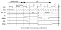
NMI Request

Bus Request

HALT Exit


Opcode fetches are compressed into just 2 clocks; the second 2 clocks of an M1 cycle are DRAM refresh, in which the Z80 puts the contents of the R register on the address bus and then increments the lower 7 bits of R.
Since opcode fetches require the memory to respond faster than normal read/write cycles do, some machines (like the MSX) have an externally-inserted wait state only on M1 cycles. Source
CPC Timings
On MSX, bus arbitration only applies to M1 machine cycles but access to VRAM has other limitations. On ZX Spectrum, bus arbitration is done not by using the /WAIT pin but by disabling the CPU clock when needed.
On CPC, bus arbitration occurs on every CPU bus access. The Gate Array asserts the /WAIT pin on the Z80 for 3 out of every 4 cycles, effectively aligning all bus operations to a 4-tick cycle. The Z80 extends T2 indefinitely by adding wait states until /WAIT is released.
The NOPs column corresponds to CPC timings, which account for the bus arbitration. The NOP instruction takes 4 cycles. This is the minimum amount of cycles an instruction can take.
Every M-cycle that involves a memory or I/O access will stretch the previous M-cycle due to bus arbitration. But beware, some M-cycles are purely internal and don't involve a memory or I/O access. So those won't stretch the previous M-cycle.
Nevertheless, a few CPC timings can appear surprising at first glance:
- Instructions LD (IX+d),r and LD (IX+d),n take 5 and 6 NOPs respectively, even though they are both listed as 19 (4,4,3,5,3) cycles in the datasheet. This happens because LD (IX+d),r has one less memory access operation to do compared to LD (IX+d),n as it does not have to fetch its operand from memory.
- Instructions IN r,(C) and OUT (C),r take 4 NOPs with CPC timings, even though they are listed as 12 (4,4,4) cycles in the datasheet. This happens because I/O access is not aligned with memory access. On Zilog manual, it is precised that one wait-state TW is automatically inserted after T2 on I/O access.
The CPC timings of some instructions will be altered if an interrupt happens. The interrupt test occurs on the last T-state of the instruction, and if it's low, the Z80 will insert 2 wait states to acknowledge the interrupt.
So, instructions which end in the third or fourth T-state relative to the read alignment for the next instruction fetch will be delayed by an extra 4 T-states. The few instructions which end in the first or second T-state won't since the first instruction fetch/read in the interrupt won't be delayed an extra 4 T-states. Source
Opcodes
The Z80 follows a 2-3-3 opcode bit pattern. Register instructions normally use three bits to specify the register used: 000=B, 001=C, 010=D, 011=E, 100=H, 101=L, 110=indirect through HL, 111=A.
Register pairs are encoded as: 00=BC, 01=DE, 10=HL, 11=SP. The PUSH and POP instructions use a slightly different encoding: 00=BC, 01=DE, 10=HL, 11=AF.
Three bits are used to specify condition codes: 000=NZ (Non Zero), 001=Z (Zero), 010=NC (Non Carry), 011=C (Carry), 100=PO (Parity Odd), 101=PE (Parity Even), 110=P (Plus), 111=M (Minus). The JR instruction only decodes the 2 lower bits of the condition code.
Condition C (carry) is unrecognizable from register C. To recognize which it is, conditions (flags) are used only in instructions: CALL, JR, JP, RET.
All CB-prefixed opcodes and half of the standard opcodes (from &40 to &BF) follow a strict uniform layout. The sole exception is the HALT instruction (opcode &76), which replaces the expected LD (HL),(HL) instruction.
The rest of the opcode table is also neatly organised but in a horizontal way instead of vertical.
Any instruction in bold is undocumented by Zilog.
Standard opcodes
|
|
|
|
|
|
|
|
|
|
|
|
|
|
|
|
|
|
|
|
|
|
|
|
|
|
|
|
|
|
|
|
CB-prefixed opcodes
|
|
|
|
|
|
|
| ||||||||||||||||||||||||||||||||||||||||||||||||||||||||||||||||||||||||||||||||||||||||||||||||||||||||||||||||||||||||||||||||||||||||||||||||
|
|
|
|
|
|
|
| ||||||||||||||||||||||||||||||||||||||||||||||||||||||||||||||||||||||||||||||||||||||||||||||||||||||||||||||||||||||||||||||||||||||||||||||||
|
|
|
|
|
|
|
| ||||||||||||||||||||||||||||||||||||||||||||||||||||||||||||||||||||||||||||||||||||||||||||||||||||||||||||||||||||||||||||||||||||||||||||||||
|
|
|
|
|
|
|
|
ED-prefixed opcodes
The opcodes that are not mentioned in the following table are EDNOP (ED-prefixed NOP instruction). Thay have no effect but take 8 cycles and increment the register R two times. EDED, EDDD, EDFD and EDCB are also EDNOP instructions.
|
|
|
|
|
|
|
| ||||||||||||||||||||||||||||||||||||||||||||||||||||||||||||||||||||||||||||||||||||||||||||||||||||||||||||||||||||||||||||||||||||||||||||||||
|
|
|
|
Notes:
- The opcode ED70 reads the port indicated by the register C without keeping the result, but it modifies the register F
- The opcode ED71 is used in many PSG players/drivers, as it's very useful for the PSG access, which sits behind the PPI. But beware, on a CMOS Z80 this opcode behaves differently. It corresponds to the instruction OUT (C),#FF instead Source
- The opcode EDFF is used by Winape (and other emulators) to break into the debugger (a 'break opcode') Source
DD or FD-prefixed opcodes
If an opcode is prefixed by DD, the instruction is changed as follows:
- HL is replaced by IX
- H is replaced by IXH
- L is replaced by IXL
- (HL) is replaced by (IX+d)
Same for the FD prefix but with IY instead of IX.
There are 3 exceptions:
- In the instruction EX DE,HL, HL will not be replaced with IX or IY. The EXX instruction is not affected either.
- If (HL) and L or H are used in the same instruction, L and H are not replaced with IXL or IXH. For instance LD L,(IX+d) stores the content of (IX+d) into L, not IXL.
- DD, ED or FD prefixes cancel the effects of immediately preceding DD or FD prefixes (those become NONI: No Op No Interrupt). In other words, ED-prefixed opcodes cannot be altered by DD or FD prefixes.
DDCB or FDCB-prefixed opcodes
When a DD or FD prefix is followed by a CB byte, the CB acts as a second prefix. A mandatory displacement byte comes next, and then the actual opcode.
If the instruction produces output other than in the flags (i.e. all except BIT), then the result gets placed both into (IX+d) or (IY+d) and into the register one would normally expect to be altered.
DDCB and FDCB-prefixed instructions only increment the R register twice. Source
Optimization
- RLA, RRA, RLCA, RRCA are essentially optimized versions, one byte smaller and one M-cycle faster, of RL A, RR A, RLC A, RRC A.
- ADD A,A is one byte smaller and one M-cycle faster than SLA A.
- Similarly, ADD HL,HL is 3 bytes smaller and one M-cycle faster than SLA L; RL H.
- DJNZ loop is one byte smaller and is as fast as DEC B; JR nz,loop on CPC.
- For a smaller conditional RST #38, use JR cc,-1. This will cause a conditional jump to the displacement byte (#FF) which is the RST #38 opcode.
- To quickly invert all bits of A, CPL is one byte shorter and one M-cycle faster than XOR #FF.
- To set A to zero, XOR A is one byte smaller and one M-cycle faster than LD A,0.
- To check if A is zero, AND A or OR A are one byte smaller and one M-cycle faster than CP 0.
- An unrolled LDI loop is faster than LDIR. The same applies to other Z80 block instructions.
- If tables are aligned to a 256-byte boundary, the contents can be accessed by placing the index in a register such as L and the table address in H. This is faster than loading the full unaligned 16-bit address and adding a 16-bit index to it, and makes accessing tables with a size of 256 bytes or less very convenient.
Oddities
- RETI and RETN are identical instructions Source. The only reason for RETI is so that some other hardware can detect the specific case of returning from the interrupt, by detecting the RETI opcode on the data bus.
- EI has a 1-instruction delay. It is necessary for doing EI/RETI without any danger of nested interrupt routines.
- At the end of an NMI service routine, the earliest moment a maskable interrupt will be triggered is at the end of the instruction following RETN. Source
- RST instructions are just a CALL instruction to a fixed address baked in the instruction itself.
- Unlike the conditional JP, CALL, RET instructions which have access to all conditions, JR is limited to NZ, Z, NC, C conditions.
- Despite what the syntax of the instructions JP (HL/IX/IY) suggests, PC will be loaded with the contents of the register itself, not the indexed value. Those instructions should be understood as JP HL/IX/IY.
- The instructions LD A,A, LD B,B, LD C,C, LD D,D, LD E,E, LD H,H and LD L,L are useless. Their existence is just a side effect of how instructions are encoded as opcodes in the CPU.
- The instructions LD (nn),HL and LD HL,(nn) exist both as standard opcodes and ED-prefixed opcodes.
- The 16-bit instructions ADD HL,ss, ADC HL,ss and SBC HL,ss exist but not the instruction SUB HL,ss.
- While the syntax of the 8-bit ADD, ADC and SBC instructions all explicitly mention the A register, the SUB instruction does not mention it. On the Zilog eZ80, the SUB instruction explicitly mention the A register.
- The Z80 has a lot of 8-bit registers but it can only really do arithmetic on the A register.
- The IN r,(C) instruction updates flags but IN A,(n) does not.
- IN r,(C) and OUT (C),r instructions syntax is misleading as these instructions actually use the full 16-bit port address contained in BC. On the Zilog eZ80, these instructions are correctly named IN, r,(BC) and OUT (BC),r.
- The Amstrad engineers chose to use the high byte of the address (register B) for chip selection instead of the low byte (register C) in I/O operations. As a result, OTIR / OTDR / INIR / INDR instructions cannot be used on Amstrad CPC for transferring or reading a sequence of values on a port, as these instructions use the B register as a counter.
- INI/IND/INIR/INDR decrease B after storing the byte from the hardware port into memory. And OUTI/OUTD/OTIR/OTDR decrease B before sending the memory byte to the hardware port. Source
- All PUSH and POP instructions utilize a 16-bit operand and the high-order byte is always pushed first and popped last. PUSH HL is PUSH H then L. POP HL is POP L then H.
- When an LDxR / CPxR / INxR / OTxR instruction is interrupted, the interrupt handler sees some flags in a different state. Source
- LD A,I and LD A,R normally copy the state of IFF2 to the Parity flag. NMOS Z80 suffers a problem whereby LD A,I and LD A,R record the state of IFF2 after it has been reset if an interrupt is delivered during that instruction. Source
- Although not mentioned in Zilog documentation, the Z80 CPU supports two types of reset: normal and special. A normal reset disables the maskable interrupt, selects interrupt mode 0, zeroes registers I & R and zeroes the program counter (PC). A special reset zeroes PC only. Furthermore, a hardware bug was discovered when the special reset occurs after a HALT instruction. Source
- Almost all Z80 inputs are sampled on a rising clock, but the /WAIT signal is sampled on a falling clock. Source
Compared behaviour
- The 6502’s Decimal (BCD) mode automatically adjusts ADC and SBC results, while the Z80 requires a DAA instruction after each BCD addition and subtraction.
- The 6502 uses only one addressing mode per instruction, while the Z80 can combine two different addressing modes within a single instruction.
- The 6502 post-decrements on PHA and pre-increments on PLA, while the Z80 pre-decrements on PUSH and post-increments on POP.
- The 6502 saves flags automatically during interrupts; while the Z80 requires PUSH AF and POP AF.
- The 6502 only updates flags that are directly relevant to the operation's result. For example, EOR doesn't conceptually involve a carry, so the Carry flag is left untouched. On the Z80, XOR always clears the Carry flag to ensure a clean flag state.
Block Diagrams

The ALU uses two temporary registers that are not directly visible to the programmer:
- The Accumulator Temporary register (ACT) holds the accumulator value while an ALU operation is performed. This allows the accumulator to be updated with the new value without causing a race condition.
- The second temporary register (TMP) holds the other argument for the ALU operation. The TMP register typically holds a value from memory or another register.

See: How the Z80's registers are implemented The 16-bit increment/decrement circuit The 4-bit ALU Z80 die-shot (zeptobars) Z80 die-shot (bercovici)
The Decode ROM (PLA)
The Z80 is based around a more complicated structure than the 6502. Here the instruction is sent through a (rather) simple decoder. The decoder is built from a PLA. Simple because 8080/Z80 code offer fewer variants (i.e. addressing modes) and is quite regular compared with a 6502. The decoder creates multiple lines for each instruction or instruction group, which are fed into the second stage.
Two counters are set up in parallel. One counting the Memory (or Machine) states (M1..M5), the other Time states (T1..T5) within (note1). With a new instruction the M counter gets reset to 1, with each M state the T counter gets reset.
The second stage of instruction decode is something that is much like another PLA, but built out of single gates (note2). The gates are set up much like a grid with the timing signals (M1..M5 & T1..T5) as horizontal input and the PLA output (instructions/instruction groups) as vertical input. The gate is built along the vertical line and combining its signal with one or more timing signals using AND/NOR logic (note3). The output of these gates are fed into the discrete logic of the execution units. Source
- note1: this internal structure is also the reason for this otherwise unusual notation used throughout all Z80 documentation.
- note2: The structure is quite similar to a gate array - except that only needed inputs/functions are cast into silicon.
- note3: CMOS offers the feature to build rather complex gates with multiple inputs in a simple way - to some extend this is maybe the most unique feature about the Z80 design.
See: ARM1, Z80, 6502 instruction sequencing compared Z80 instruction decode PLA table Script processing the PLA table
CPU Pinout

- RFSH = outputs a signal to allow for memory to be refreshed
- M1 = Z80 is fetching next instruction from memory
- RESET = used to reset the Z80
- BUSRQ = Bus Request (used by external devices to request control)
- WAIT = makes the the Z80 wait during a read or write operation
- BUSACK = Bus Acknowledge – signals when Z80 is ready to hand over control
- WR = signals a memory or I/O write operation
- RD = signals a memory or I/O read operation
- INT = hardware interrupt occurred
- NMI = Non Maskable Interrupt (higher priority than the INT)
- HALT = Z80 is in a halted state
- MREQ = Z80 wants to access memory
- IORQ = Z80 wants to access an I/O port
See: Why Z80's data pins are scrambled
Chip Variants
IC Models used in CPC
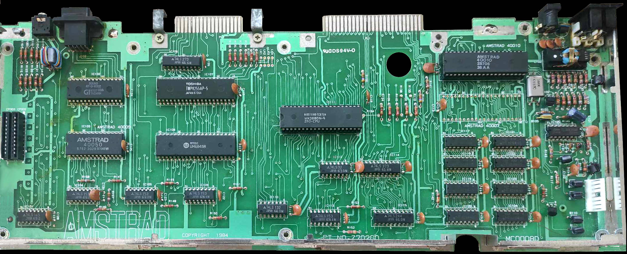
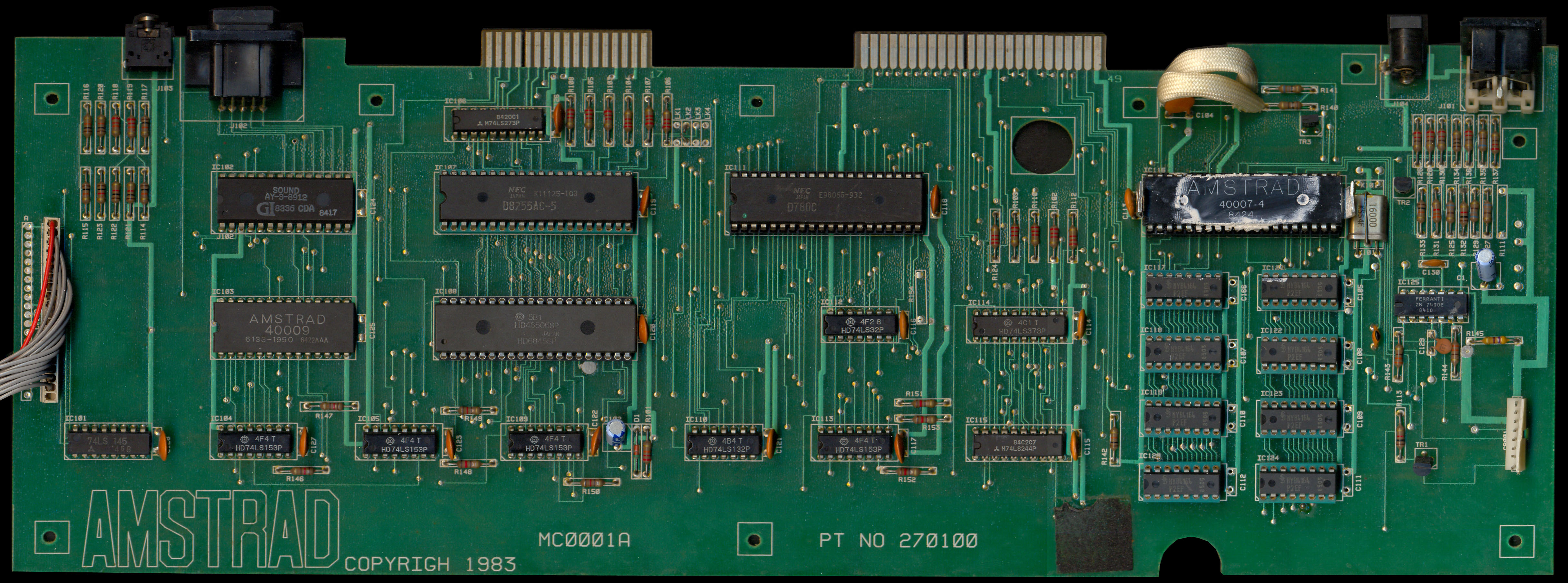
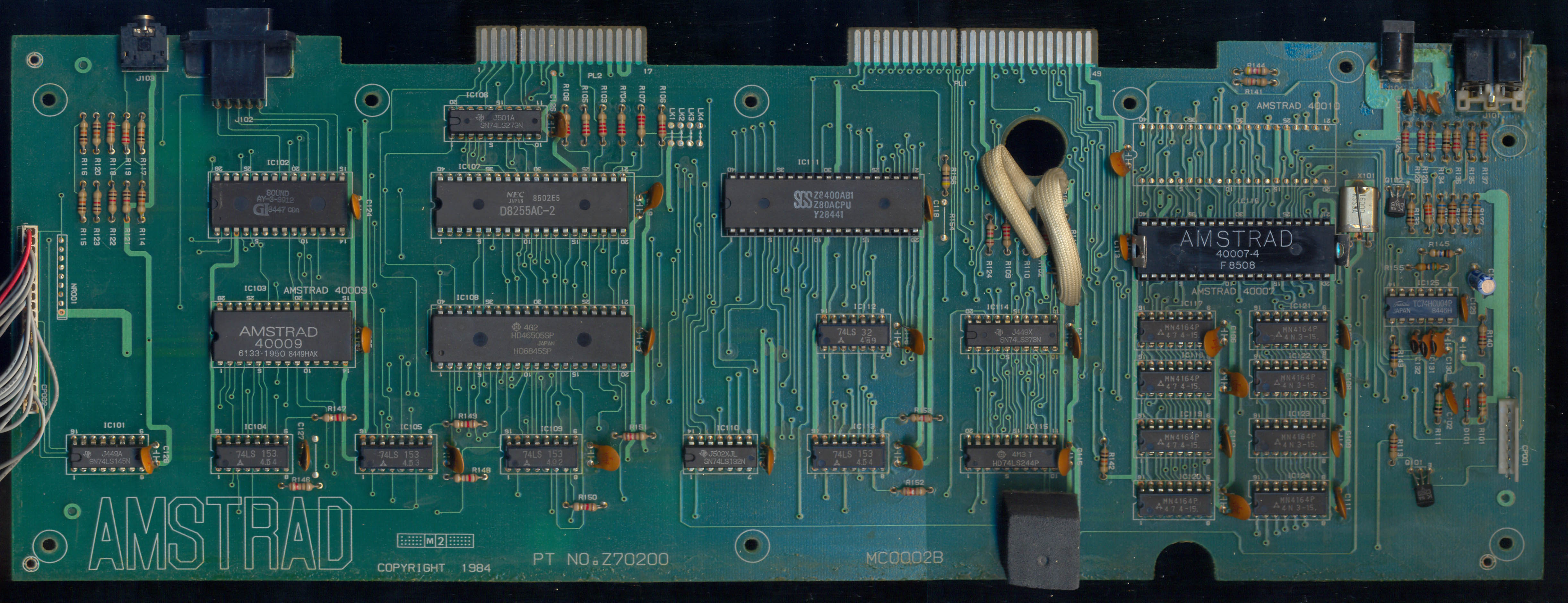
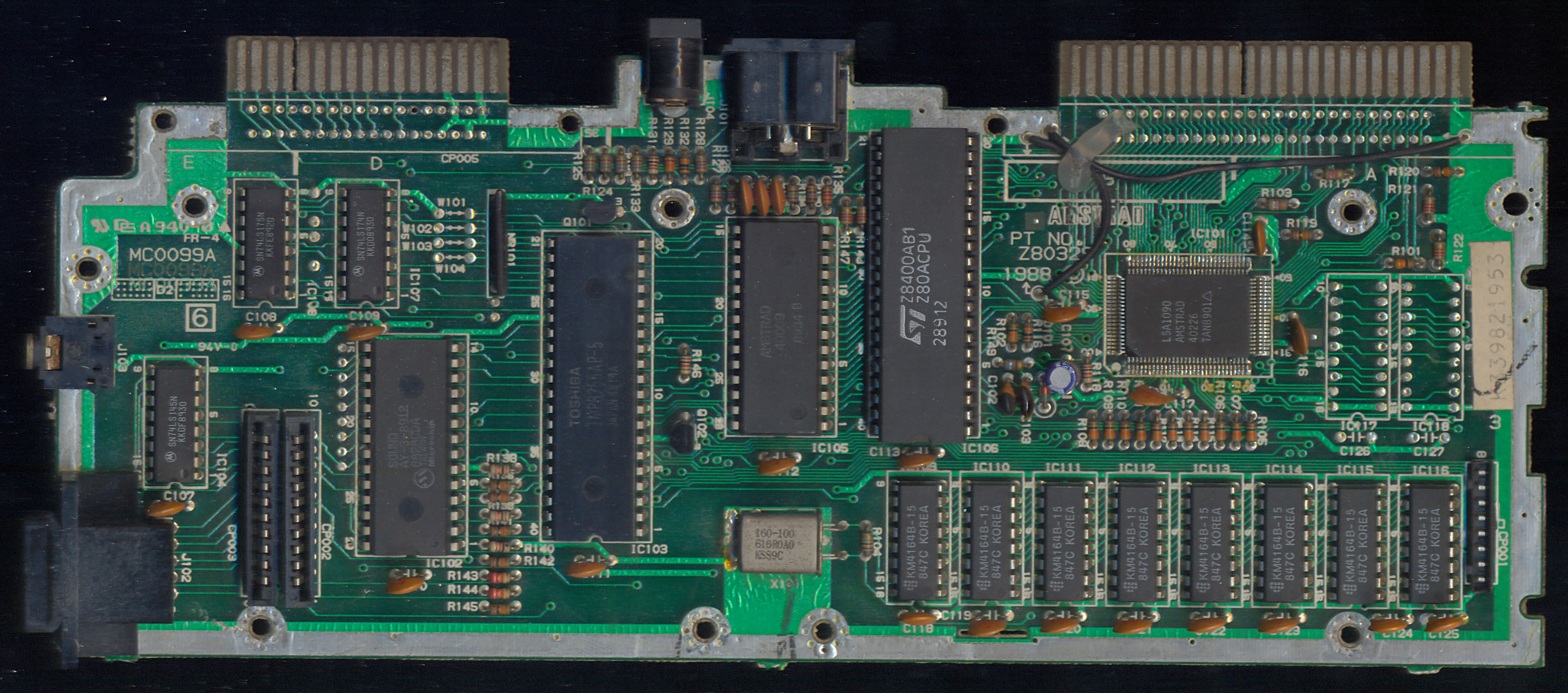
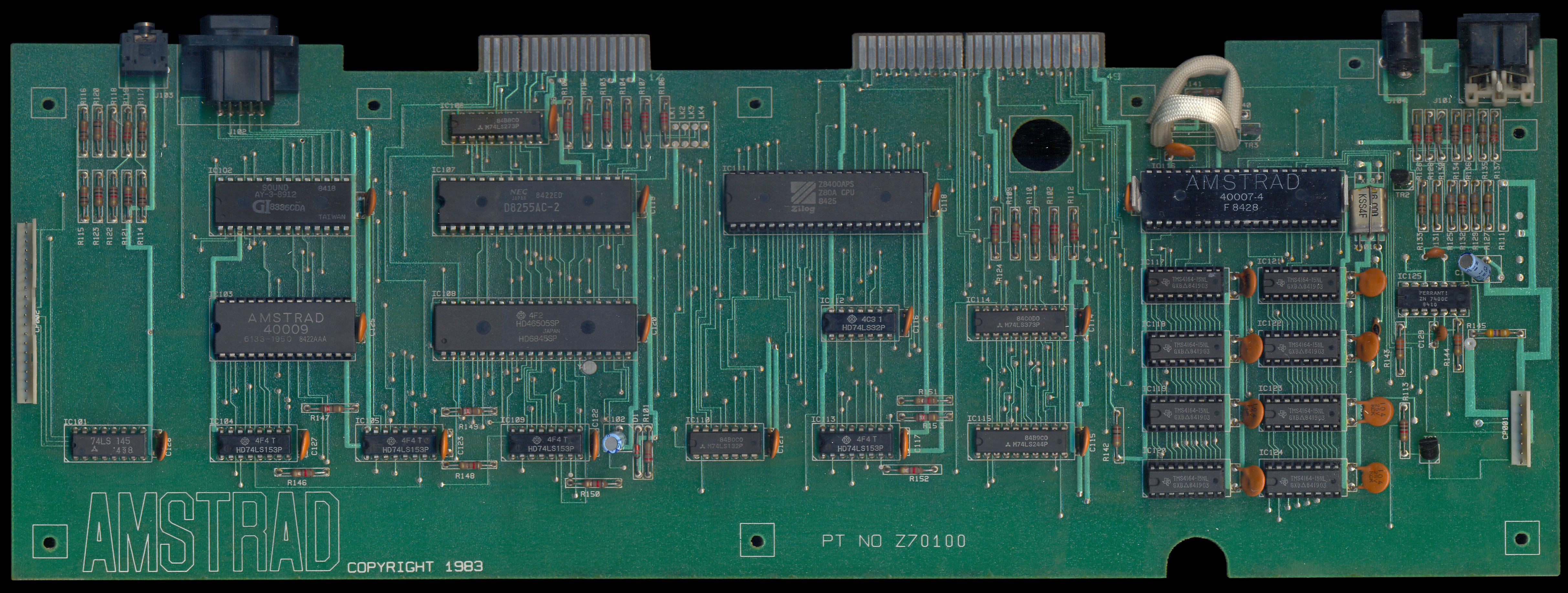
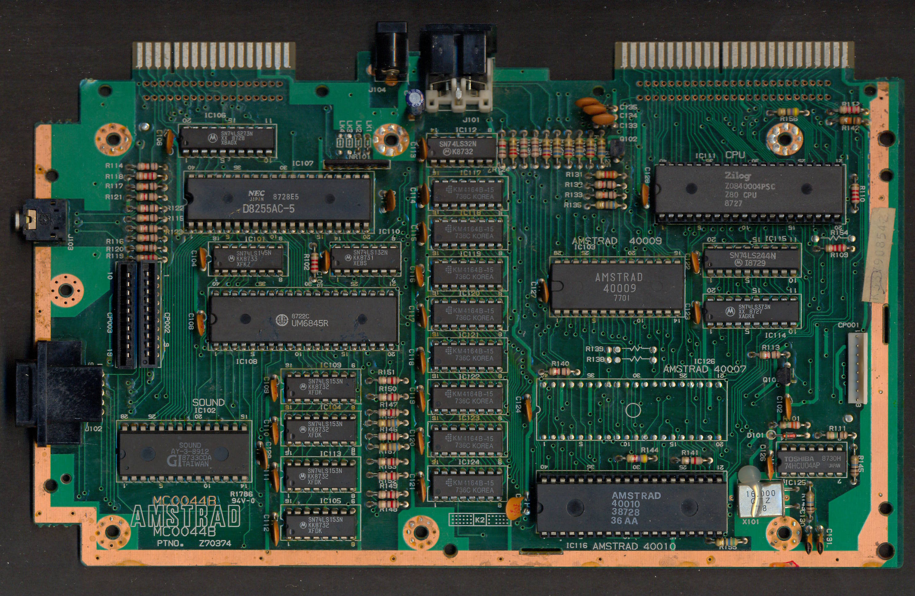
The Z80 CPU has been manufactured by others, and various Z80s have been used in the construction of the CPC during its lifetime:
- Mostek MK3880N-4 Source
- NEC D780C Source
- SGS Z8400AB1 Source
- ST Z8400AB1 Source
- Zilog Z8400APS Source
- Zilog Z0840004PSC Source
All the Z80 CPUs that Amstrad used on CPC and Plus machines are NMOS. Source
Modern incarnations
Zilog ended the production of the Z80 in April 2024. This chip is still available in ample quantities through NOS chip suppliers and can be purchased for 1.20€. Source
Zilog continues to produce the eZ80 processor, a binary-compatible upgrade of the Z80, which runs at up to 50MHz but performs like a 150MHz Z80 due to being 3 times faster at the same clock speed.
Emulation
Apart from surplus/new Z80-clones that are quite easy to find, many emulations depend on software implementations of the Z80:
- libZ80 Ultra accurate ANSI C implementation
- arnold uses InkZ80, written in C++ (taken from the InkSpector ZX Spectrum emulator)
- A-Z80 Ultra accurate Verilog implementation A-Z80 Timing Table
Other Variants
The GBZ80 (Sharp SM83) that powers the original Nintendo Gameboy and Gameboy Color is kind of an in-between the Intel 8080 and Z80. GBZ80 opcodes
The Sega Mega Drive, Master System and Game Gear use a standard Z80 CPU. Genesis sound software manual Master System reference manual Game Gear reference manual
The KC Compact uses the U880, which is an unlicensed clone of the Z80 manufactured by MME. It was the most widely used microprocessor in the German Democratic Republic. Source
The КМ1582ВМ is a Soviet clone of the Z80. It is used in the Aleste 520EX clone of the Amstrad CPC computer.
The ASCII R800 that powers the MSX TurboR is a seriously beefed up version of the Z80:
- The ALU of the R800 is 16-bit instead of 4-bit for the Z80. This change allows instructions that were being executed in 4 cycles to be done in 1 cycle.
- The instruction set of the R800 is almost identical to the Z80. Only 2 instructions have been added: MULUB and MULUW. And many of the undocumented instructions of the Z80 were made official.
Manuals
- Z80 Family Databook Z80 CPU Peripherals
- Zilog Z80 User Manual (2016)
- Zilog Z80 Technical Manual
- Mostek Z80 Programming Manual
- Mostek Z80 Technical Manual Text version - provides a detailed breakdown of the machine cycles
- Mostek Z80 Micro-Reference Manual
- Media:Z80 CPU Instant Reference Card (Color).pdf
- Media:Z80 CPC Timings cheat sheet.20230709.pdf
- Rodnay Zaks Programming the Z80 Z80 Hardware Organization
- ZX-PK forum topic on reverse engineering the Z80 (RU)
- MEMPTR, esoteric register of the Z80 CPU inir/indr/otir/otdr instructions and MEMPTR
- Z80 - undocumented opcodes
- Instruction List with T-States
Weblinks
- Z80 at the English-language Wikipedia
- Zilog Company's website
- Home of the Z80 CPU
- Zilog Z80 oral history panel
- Z80 article on Sinclair Wiki
- Learn Assembly Programming with ChibiAkumas Multi-platform Z80 tutorial
- Z80 documentation from Grimware
- Interrupt behaviour of the Z80 CPU
- Behaviour of the undocumented flags
- Zilog Z80 instruction set
- Z80 CPU instruction set database
- Decoding Z80 opcodes
- Z80 Explorer
- VisualZ80remix Detailed look at Z80 instruction timings with the help of a Z80 netlist simulation
- Cycle-stepped Z80 emulation how-to Internal Z80 behaviour described in Yaml format
- Tom Harte's SingleStepTests